Selective plasma etch of top electrodes for metal-insulator-metal (MIM) capacitors

a top electrode and capacitor technology, applied in the field of integrated circuits and ic fabrication, can solve the problems of lateral undercutting of the dielectric layer relative to the top electrode layer, adversely affecting the performance of the mim capacitor, precision and matching, and add process complexity, etc., to achieve improved capacitor critical dimension control, simplified process integration, and high selectivity

Active Publication Date: 2010-11-04
TEXAS INSTR INC
View PDF5 Cites 24 Cited by
  • Summary
  • Abstract
  • Description
  • Claims
  • Application Information

AI Technical Summary

Benefits of technology

[0006]Embodiments of the inventions describe new semiconductor etch processes that comprise at least in part dry (e.g., plasma) etching of the top electrode of MIM capacitors, and ICs therefrom. Such processes generally provide high selectivity to the underlying dielectric (e.g., >8, such as ≧10), which is generally a thin dielectric (e.g., <1,000 A, typically <400A) and improved capacitor critical dimension (CD) control. For embodiments of the invention where the top electrode layer etch is exclusively dry-etched, such embodiments generally allow simplified process integration by eliminating the need for the hard mask (e.g., silicon nitride) needed for top electr

Problems solved by technology

Known reasonably selective top electrode etch chemistries generally comprise at least in part wet etching, which necessitates the use of hard masking layers (e.g., silicon nitride), which adds to process complexity, cycle time and cost as compared to soft masking (resist) layers which can be used with dry (e.g., plasma) etch processes.
In contrast, due to the isotropic nature of wet etching, the wet etch

Method used


Image

  • Selective plasma etch of top electrodes for metal-insulator-metal (MIM) capacitors
  • Selective plasma etch of top electrodes for metal-insulator-metal (MIM) capacitors
  • Selective plasma etch of top electrodes for metal-insulator-metal (MIM) capacitors

Examples


example 1

[0033]A MIM capacitor was formed on a bulk silicon test wafer and the top electrode was defined by an Applied Materials (Santa Clara, Calif.) DPS™ etcher. The bottom electrode layer of the MIM capacitor comprised aluminum, the dielectric comprised a 250 A thick dielectric stack comprising silicon oxide / SiON / silicon oxide, and the top electrode layer comprised 1,800 A of TiN. The etch gases comprised Cl2=90 sccm, Ar=10 sccm, CHF3=10 sccm, and other etch parameters comprised a chamber pressure=15 mtorr, cathode 45° C., backside He pressure=10 T, power 25 W bias, and an 800 W RF source. The TiN:oxide selectivity was found to be ≧10:1 and the TiN etch rate was found to be about 1,800 A / min. A 365 nm wavelength (near ultra-violet (NUV)) was used to allow the TiN etch to endpoint on the thin silicon oxide layer.

example 2

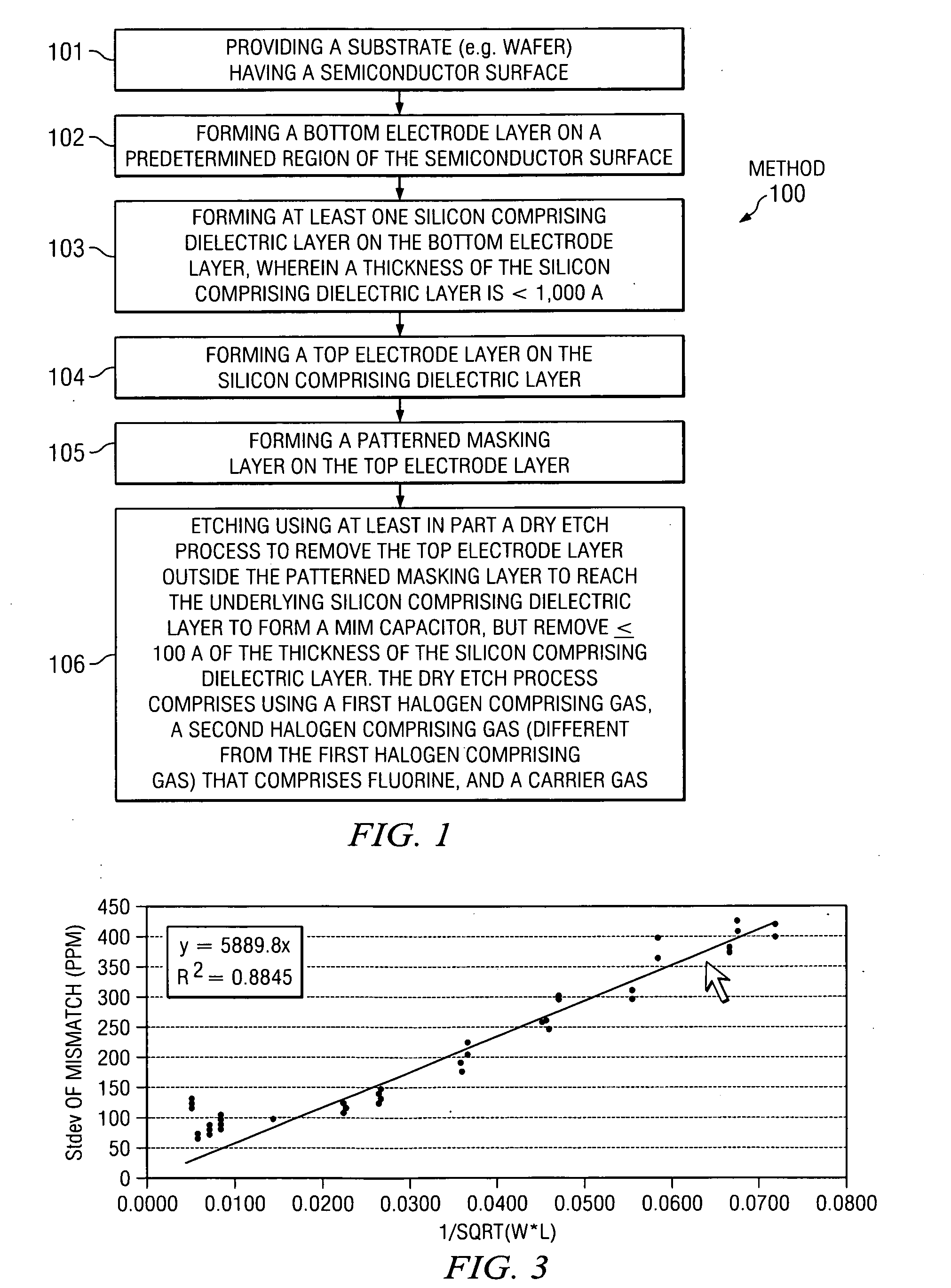
[0034]An IC having a plurality of MIM capacitors was formed having the MIM capacitor structure and using a dry-etch only top electrode layer etch process as described immediately above. FIG. 3 shows MIM capacitor match data demonstrating capacitor matching of about 200 ppm-μm for MIM capacitors having W=L=37 μm, according to an embodiment of the invention. In comparison, for the same geometry, MIM capacitors formed using a conventional dry+wet top electrode layer etch were found to provide matching of 300-400 ppm-μm. The significant improvement in MIM capacitor matching for MIM capacitors according to embodiments of the invention is provided primarily because the dry-etch controls the CD of the MIM capacitors more tightly as compared to conventional dry+wet etch combination as described above.

[0035]Embodiments of the invention can be integrated into a variety of process flows to form a variety of devices and related products. The semiconductor substrates may include various elements...


PUM


Abstract

A method of forming integrated circuits (IC) having at least one metal insulator metal (MIM) capacitor. A bottom electrode is formed on a predetermined region of a semiconductor surface of a substrate. At least one dielectric layer including silicon is formed on the bottom electrode, wherein a thickness of the dielectric layer is <1,000 A. A top electrode layer is formed on the dielectric layer. A patterned masking layer is formed on the top electrode layer. Etching using dry-etching at least in part is used to etch the top electrode layer outside the patterned masking layer to reach the dielectric layer, which removes ≦100 A of the thickness of the dielectric layer. The dry etch process includes using a first halogen comprising gas, a second halogen comprising gas that comprises fluorine, and a carrier gas.

Description

FIELD OF THE INVENTION[0001]Embodiments of the invention are related to integrated circuits (ICs) and IC fabrication, and more particularly to ICs including metal-insulator-metal (MIM) capacitors, and fabrication methods thereof.BACKGROUND[0002]One type of passive component that is increasingly incorporated into many IC designs is a MIM capacitor, which typically incorporates a stacked arrangement of materials that comprises top and bottom electrically conductive electrodes, and an intermediate insulator layer incorporating one or more dielectric layers. Typically, a MIM capacitor is fabricated between metal interconnect layers in an IC (e.g., between the M2 and M3 layer), which locates the MIM capacitor away from the underlying semiconductor surface, such that parasitic capacitance effects with the semiconductor surface of the substrate are minimized.[0003]Given the ever-present desire to reduce the sizes of components in an IC, it is desirable to minimize the circuit area occupied...

Claims


Application Information

Patent Timeline
IPC IPC(8): H01L27/10H01L21/66H01L21/02
CPCH01L22/26H01L28/40H01L27/0805
Inventor CATHEY, MARSHALL O.MAHALINGAM, PUSHPATIAN, WEIDONGGUILING, DAVID C.CHEN, XINFENHU, BINGHUACHEVACHAROENKUL, SOPA
Owner TEXAS INSTR INC
Why Eureka
Try Eureka