

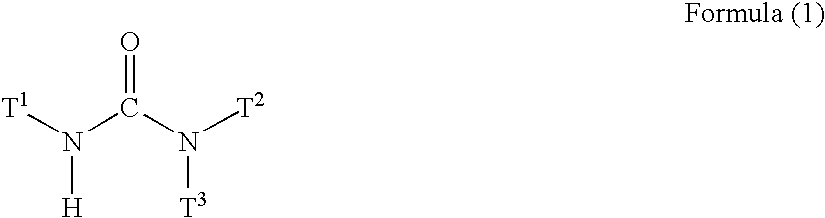
Silicon-containing resist underlayer film forming composition having urea group
a technology of underlayer film and composition, which is applied in the direction of photomechanical equipment, instruments, photosensitive material processing, etc., can solve the problem of large influence of activating light ray reflection on semiconductor substrates
- Summary
- Abstract
- Description
- Claims
- Application Information
AI Technical Summary
Benefits of technology
Problems solved by technology
Method used
Image


Examples
synthesis example 1
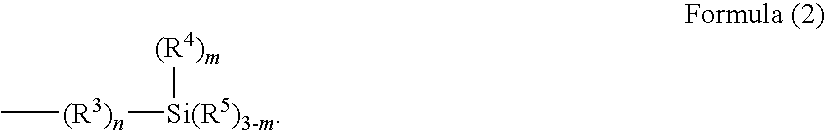
[0161]0.95 g of 1-[3-(trimethoxysilyl)propyl]urea (Formula III-1), 57.41 g of tetraethoxysilane, 23.03 g of methyltriethoxysilane, 4.27 g of phenyltrimethoxysilane, and 85.67 g of ethanol were charged into a 300 mL flask to be dissolved and the resultant mixed solution was warmed while stirring the mixed solution with a magnetic stirrer to reflux. Next, an aqueous solution in which 0.50 g of maleic acid was dissolved in 28.23 g of ion-exchanged water, was added to the mixed solution. After the reaction was effected for 120 minutes, the resultant reaction solution was cooled down to room temperature. Subsequently, 100 g of propylene glycol monomethyl ether acetate and 100 g of propylene glycol-n-monopropyl ether were added to the reaction solution, and ethanol and water as reaction by-products were distilled off under reduced pressure to produce a solution of a hydrolysis-condensation product. The weight average molecular weight Mw of the obtained polymer (Formula IV-31) was measured...
synthesis example 2
[0162]2.39 g of 1-[3-(trimethoxysilyl)propyl]urea (Formula III-1), 56.04 g of tetraethoxysilane, 23.02 g of methyltriethoxysilane, 4.27 g of phenyltrimethoxysilane, and 85.72 g of ethanol were charged into a 300 mL flask to be dissolved and the resultant mixed solution was warmed while stirring the mixed solution with a magnetic stirrer to reflux. Next, an aqueous solution in which 0.50 g of maleic acid was dissolved in 28.23 g of ion-exchanged water, was added to the mixed solution. After the reaction was effected for 120 minutes, the resultant reaction solution was cooled down to room temperature. Subsequently, 100 g of propylene glycol monomethyl ether acetate and 100 g of propylene glycol-n-monopropyl ether were added to the reaction solution, and ethanol and water as reaction by-products were distilled off under reduced pressure to produce a solution of a hydrolysis-condensation product. The weight average molecular weight Mw of the obtained polymer (Formula IV-31) was measured...
synthesis example 3
[0163]4.54 g of 1-[3-(trimethoxysilyl)propyl]urea (Formula III-1), 57.41 g of tetraethoxysilane, 21.86 g of methyltriethoxysilane, 4.05 g of phenyltrimethoxysilane, and 85.78 g of ethanol were charged into a 300 mL flask to be dissolved and the resultant mixed solution was warmed while stirring the mixed solution with a magnetic stirrer to reflux. Next, an aqueous solution in which 0.47 g of maleic acid was dissolved in 27.96 g of ion-exchanged water, was added to the mixed solution. After the reaction was effected for 120 minutes, the resultant reaction solution was cooled down to room temperature. Subsequently, 100 g of propylene glycol monomethyl ether acetate and 100 g of propylene glycol-n-monopropyl ether were added to the reaction solution, and ethanol and water as reaction by-products were distilled off under reduced pressure to produce a solution of a hydrolysis-condensation product. The weight average molecular weight Mw of the obtained polymer (Formula IV-31) was measured...
PUM
| Property | Measurement | Unit |
|---|---|---|
| Composition | aaaaa | aaaaa |
| Hydrolysable | aaaaa | aaaaa |
Abstract
Description
Claims
Application Information