Enhancement of organic photovoltaic cell open circuit voltage using electron/hole blocking exciton blocking layers

an organic photovoltaic cell and exciton blocking technology, applied in thermoelectric devices, solid-state devices, nano-informatics, etc., can solve the problems of difficult and expensive production of efficient crystalline-based devices, low power conversion efficiency of photosensitive optoelectronic devices, and low efficiency of crystalline-based devices. achieve the effect of increasing the open circuit voltage of the device, reducing the dark current, and increasing the power conversion efficiency of the devi

Inactive Publication Date: 2011-01-20
RGT UNIV OF MICHIGAN
View PDF4 Cites 73 Cited by
  • Summary
  • Abstract
  • Description
  • Claims
  • Application Information

AI Technical Summary

Benefits of technology

[0049]The present disclosure is further directed to a method of increasing the power conversion efficiency of a photosensitive optoelectronic device comprising incorpo

Problems solved by technology

As a general rule, a photovoltaic cell provides power to a circuit, device or equipment, but does not provide a signal or current to control detection circuitry, or the output of information from the detection circuitry.
In contrast, a photodetector or photoconductor provides a signal or current to control detection circuitry, or the output of information from the detection circuitry but does not provide power to the circuitry, device or equipment.
However, efficient crystalline-based devices, especially of large surface area, are difficult and expensive to produce due to the problems inherent in producing large crystals without significant efficiency-degrading defects.
On the other hand, high efficiency amorphous silicon devices still suffer from problems wit

Method used


Image

  • Enhancement of organic photovoltaic cell open circuit voltage using electron/hole blocking exciton blocking layers
  • Enhancement of organic photovoltaic cell open circuit voltage using electron/hole blocking exciton blocking layers
  • Enhancement of organic photovoltaic cell open circuit voltage using electron/hole blocking exciton blocking layers

Examples


example 1

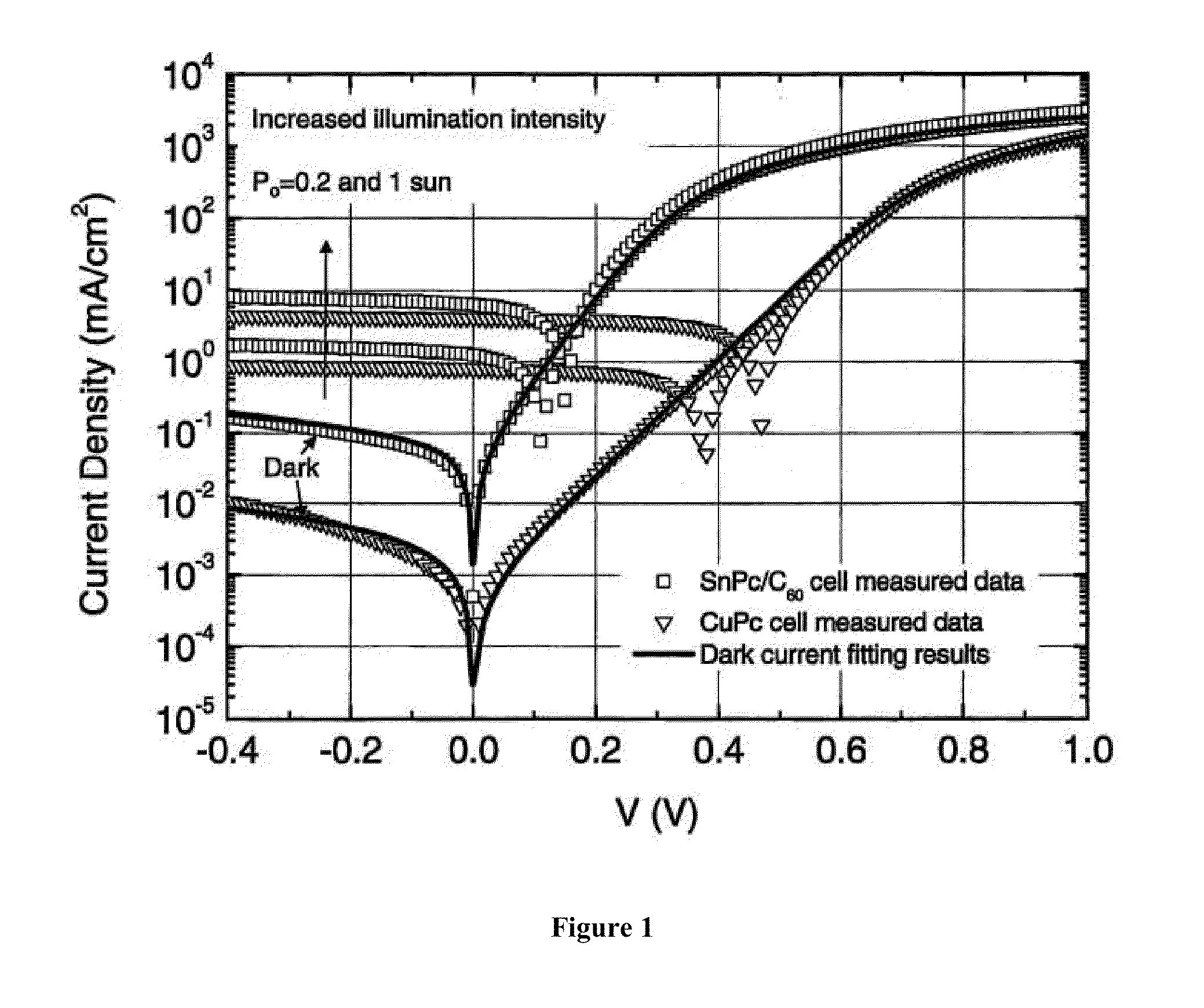
[0098]Devices were prepared on 1500-Å-thick layers of ITO (sheet resistance of 15 Ω / cm2) precoated onto glass substrates. The solvent-cleaned ITO surface was treated in ultraviolet / O3− for 5 min immediately before loading into a high vacuum chamber (base pressure −7 Torr), where the organic layers and a 100-Å-thick Al cathode were sequentially deposited via thermal evaporation. The deposition rate of the purified organic layers was ˜Å / s. (Laudise et al., J. Cryst. Growth, 187, 449 (1998).) The Al cathode was evaporated through a shadow mask with 1 mm-diameter openings to define the device active area. The current density versus voltage (J-V) characteristics were measured in the dark and under simulated AM1.5G solar illumination. Illumination intensity and quantum efficiency measurements were conducted using standard methods employing an NREL calibrated Si detector. (ASTM Standards E1021, E948, and E973, 1998.)

[0099]FIG. 1 shows the current density-voltage (J-V) characteristics of an...

example 2

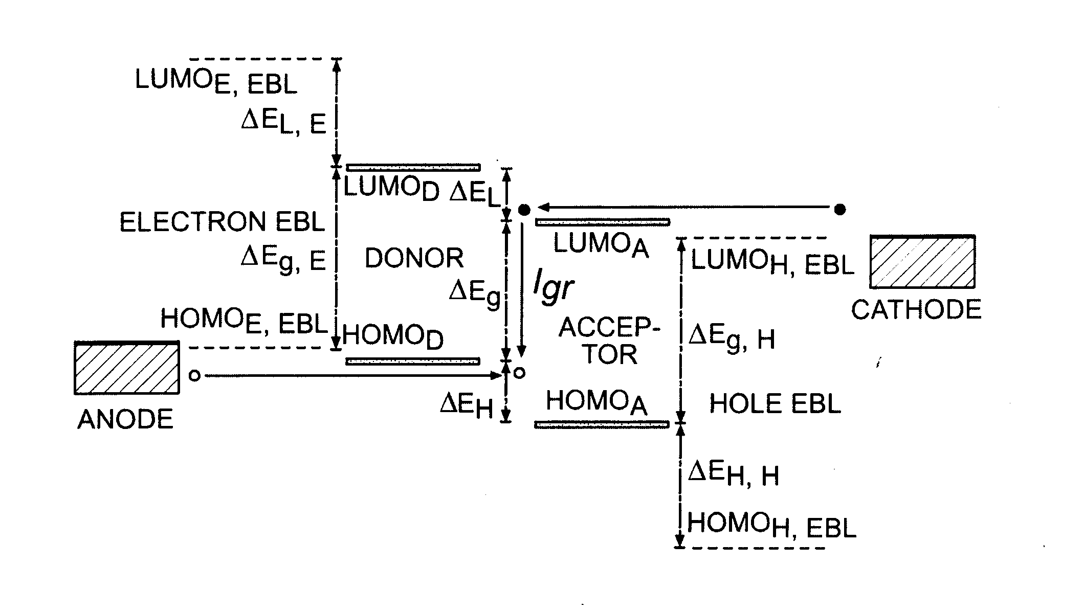
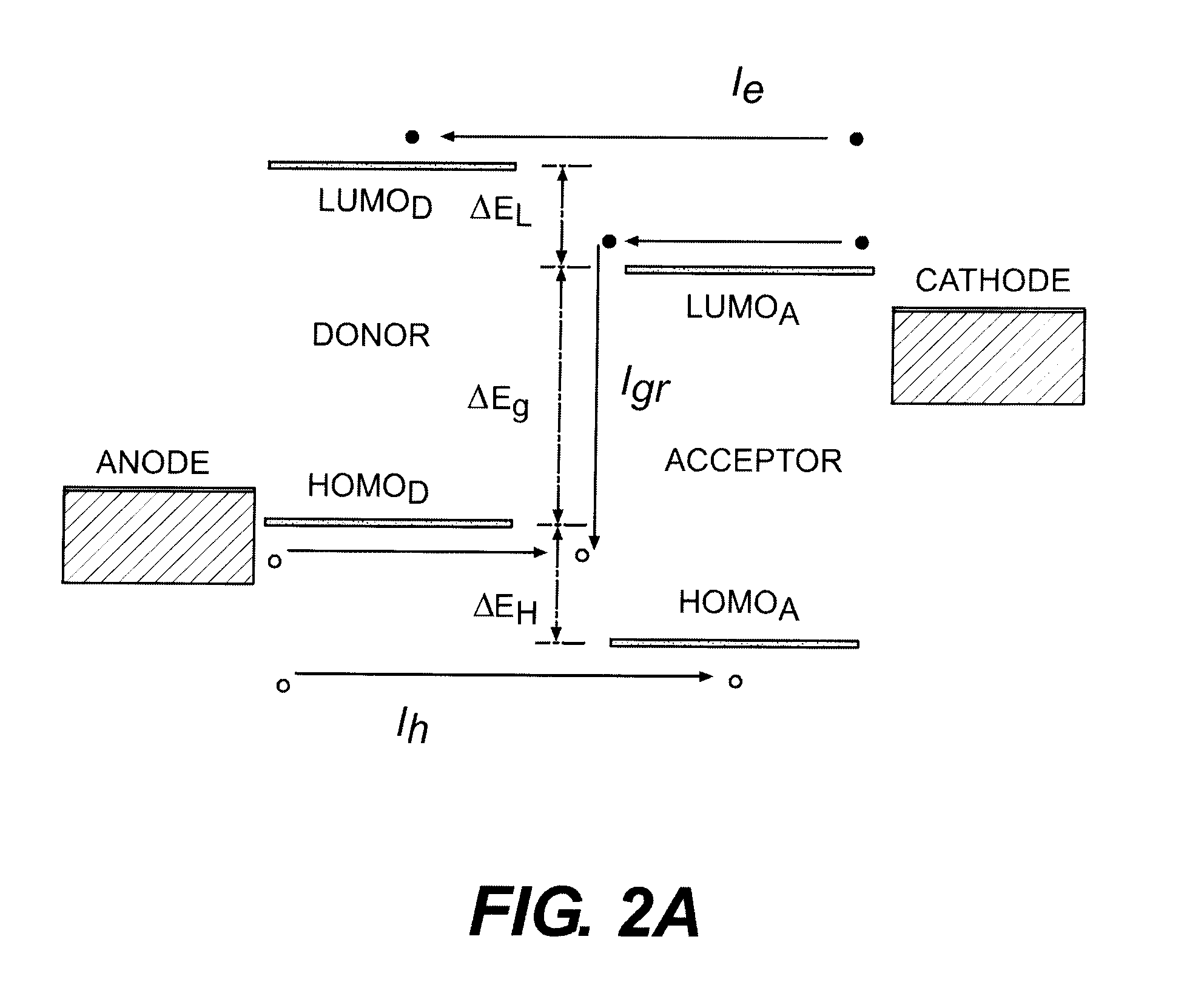
[0101]To decrease JS, and hence increase VOC in a SnPc / C60 cell, an electron blocking EBL was inserted between the anode and the SnPc donor layer described in Example 1. According to the energy level diagram in the inset of FIG. 2, the electron blocking EBL should (i) have a higher LUMO energy than the donor LUMO, (ii) have a relatively high hole mobility, and (iii) limit dark current due to generation and recombination at the interface with the donor resulting from a small electron blocking EBL (HOMO) to donor (LUMO) “interfacial gap” energy. Following these considerations, the inorganic material MoO3, and boron subphthalocyanine chloride (SubPc) and CuPc were employed as electron blocking EBLs. (Mutolo et al., J. Am. Chem. Soc., 128, 8108 (2006)) According to their respective energy levels (FIG. 2), they all effectively impede electron current from the donor to the anode contact. MoO3 has previously been used in polymer PV cells to prevent reactions between ITO and the polymer PV ...


PUM


Abstract

The present disclosure relates to photosensitive optoelectronic devices comprising at least one of an electron blocking or hole blocking layer. Further disclosed are methods of increasing power conversion efficiency in photosensitive optoelectronic devices using at least one of an electron blocking or hole blocking layer. The electron blocking and hole blocking layers presently disclosed may reduce electron leakage current by reducing the dark current components of photovoltaic cells. This work demonstrates the importance of reducing dark current to improve power conversion efficiency of photovoltaic cells.

Description

CROSS-REFERENCE TO RELATED APPLICATION[0001]This application claims priority to U.S. Provisional Application No. 61 / 144,043, filed on Jan. 12, 2009, which is incorporated herein by reference in its entirety.STATEMENT REGARDING FEDERALLY SPONSORED RESEARCH[0002]This invention was made with U.S. Government support under FA9550-07-1-0364 awarded by the U.S. Air Force Office of Scientific Research, and DE-FG36-08GO18022 awarded by the U.S. Department of Energy. The government has certain rights in the invention.JOINT RESEARCH AGREEMENT[0003]The claimed invention was made by, on behalf of, and / or in connection with one or more of the following parties to a joint university-corporation research agreement: University of Michigan and Global Photonic Energy Corporation. The agreement was in effect on and before the date the invention was made, and the claimed invention was made as a result of activities undertaken within the scope of the agreement.FIELD OF THE DISCLOSURE[0004]The present dis...

Claims


Application Information

Patent Timeline
IPC IPC(8): H01L51/42
CPCB82Y10/00Y02E10/549H01L51/424H01L51/0048H10K85/221H10K30/20H10K30/50H10K30/30H10K30/353H10K85/211H10K30/81H10K30/00H10K85/324H10K85/311H10K85/623H10K85/621H10K85/342H10K85/40H10K85/60H10K85/381
Inventor FORREST, STEPHEN R.LI, NING
Owner RGT UNIV OF MICHIGAN
Why Eureka
Try Eureka