Superior fill conditions in a replacement gate approach by using a tensile stressed overlayer

a filling condition and overlayer technology, applied in the direction of transistors, electrical apparatus, semiconductor devices, etc., can solve the problems of a large influence of the conductivity of the channel region on the performance of the mos transistor, increased leakage current, and pronounced dependence of the threshold voltage on the channel length, so as to reduce the strain-inducing effect of the tensile stressed dielectric material

Active Publication Date: 2011-03-03
GLOBALFOUNDRIES US INC
View PDF5 Cites 16 Cited by
  • Summary
  • Abstract
  • Description
  • Claims
  • Application Information

AI Technical Summary

Benefits of technology

[0017]A further illustrative method disclosed herein comprises forming a tensile stressed dielectric material so as to laterally enclose a gate electrode structure of a transistor and to expose a top surface of a placeholder material of the gate electrode structure. Furthermore, the method comprises removing the placeholder material in the presence of the tensile stressed

Problems solved by technology

Hence, the conductivity of the channel region substantially affects the performance of MOS transistors.
The short channel behavior may lead to an increased leakage current and to a pronounced dependence of the threshold voltage on the channel length.
Aggressively scaled transistor devices with a relatively low supply voltage and thus reduced threshold voltage may suffer from an exponential increase of the leakage current, while also requiring enhanced capacitive coupling of the gate electrode to the channel region.
Although, generally, usage of high speed transistor elements having an extremely short channel may be substantially restricted to high speed signal paths, whereas transistor elements with a longer channel may be used for less critical signal paths, such as storage transistor elements, the relatively high leakage current caused by direct tunneling of charge carriers through an ultra-thin silicon dioxide gate insulation layer may reach values for an oxide thickness in the range or 1-2 nm that may not be compatible with thermal design power requirements for performance driven circuits.
Providing different metal species for adjusting the work function of the gate electrode structures for P-channel transistors and N-channel transistors at an early manufacturing stage may, however, be associated with a plurality of difficulties, which may stem from the fact that a complex patterning sequence may be required during the formation of the sophisticated high-k metal gate stack, which may result in a significant variability of the resulting work function and thus threshold of the completed transistor structures.
For instance, during a corresponding manufacturing

Method used


Image

  • Superior fill conditions in a replacement gate approach by using a tensile stressed overlayer
  • Superior fill conditions in a replacement gate approach by using a tensile stressed overlayer
  • Superior fill conditions in a replacement gate approach by using a tensile stressed overlayer

Examples


Embodiment Construction

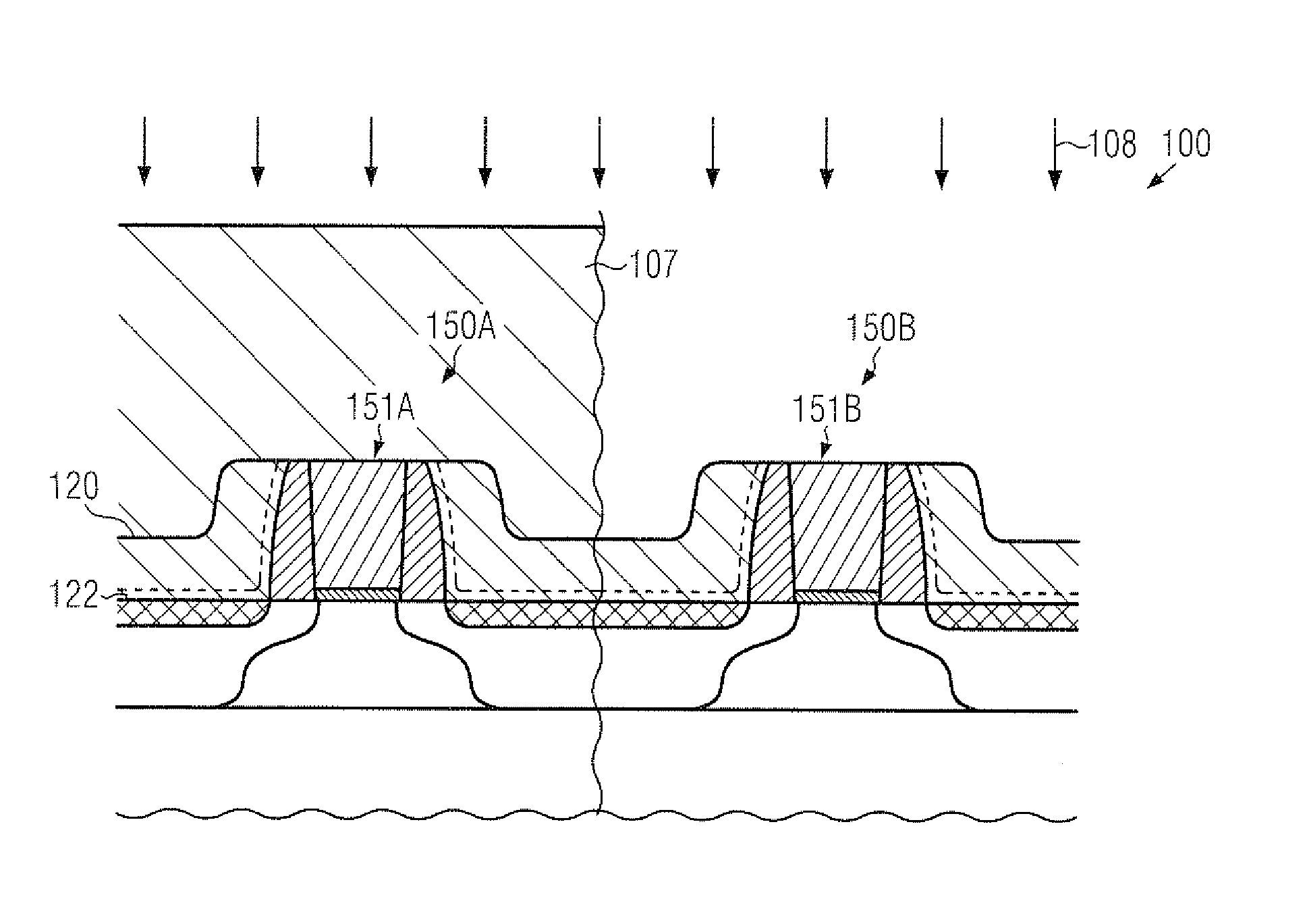
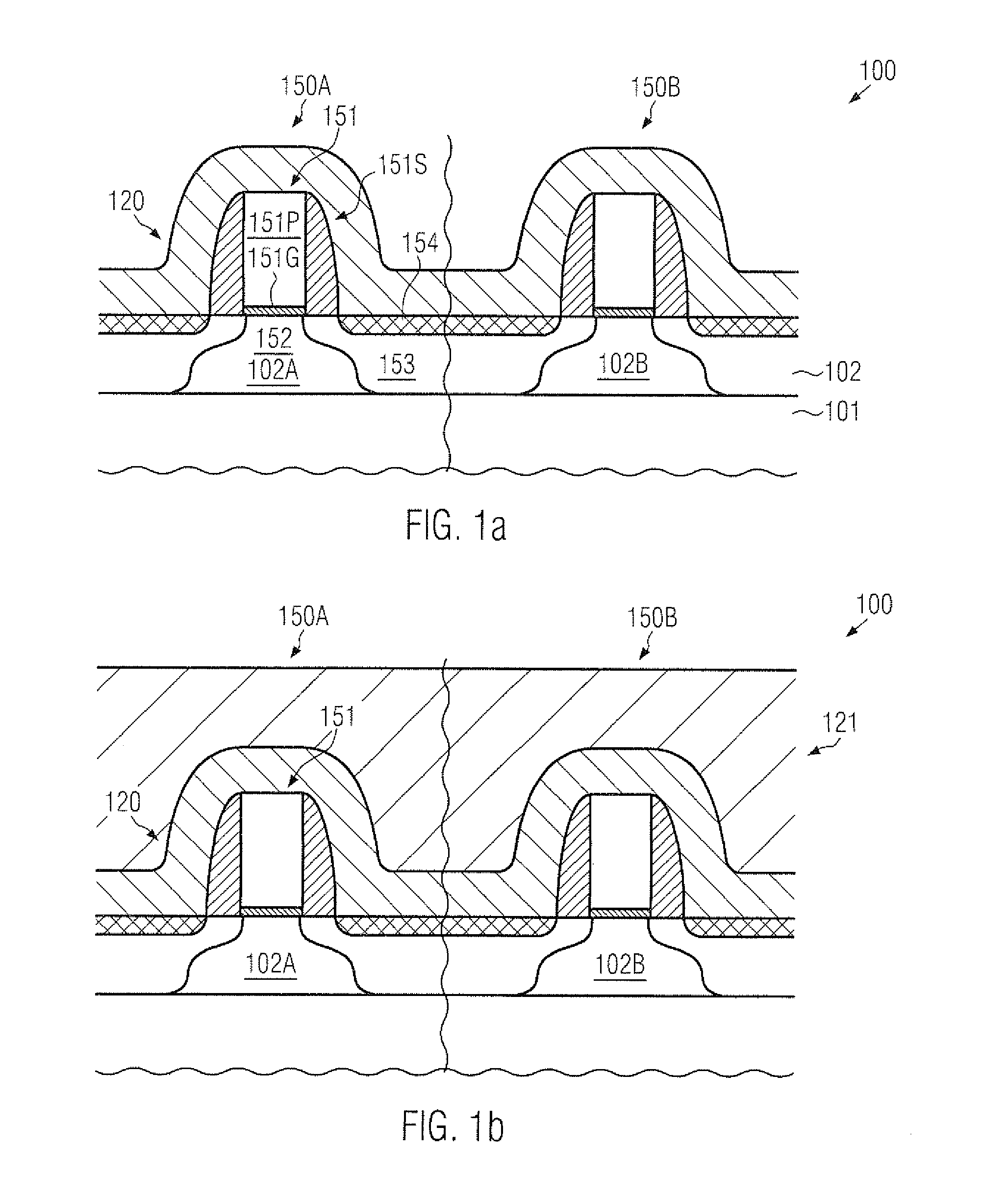
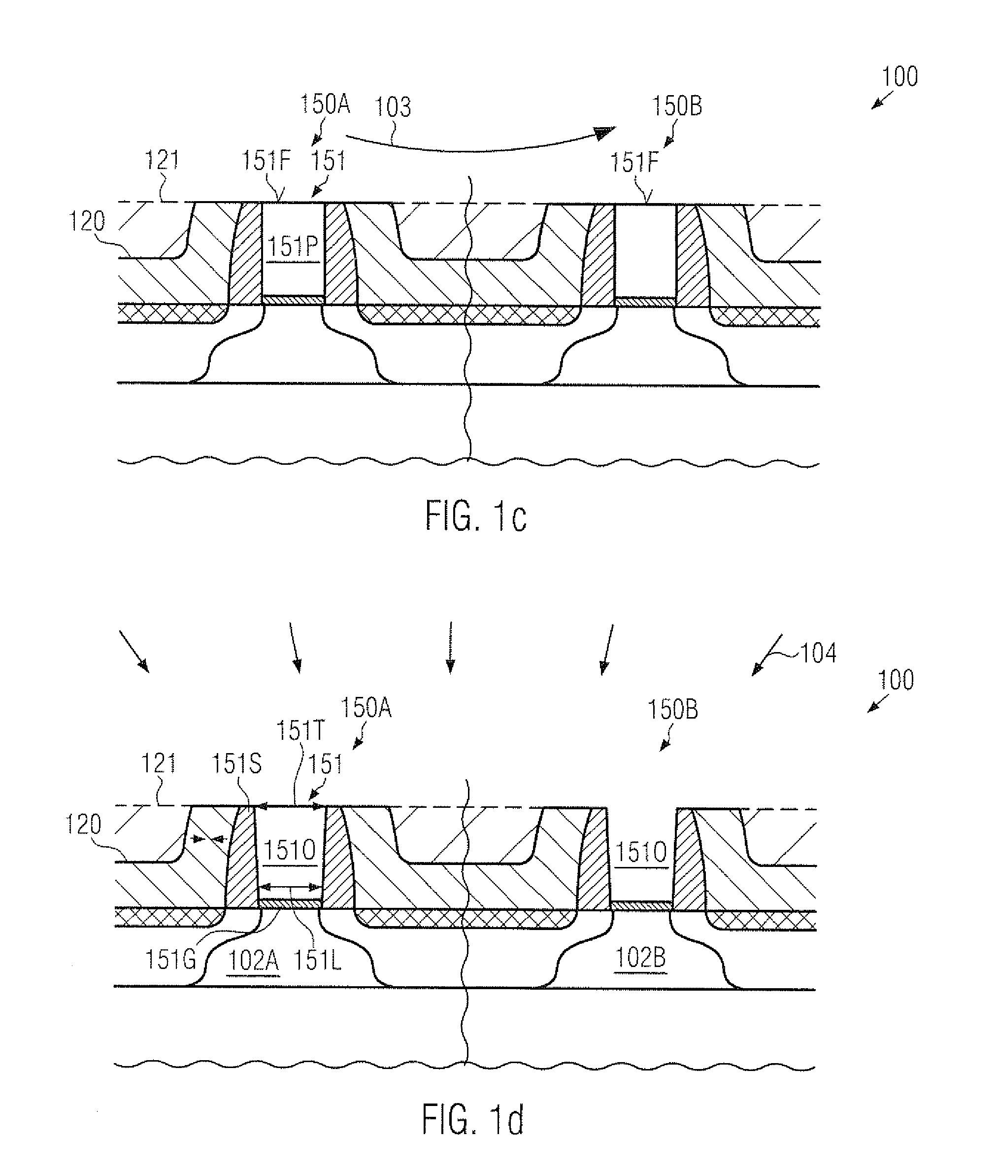
[0024]Various illustrative embodiments of the invention are described below. In the interest of clarity, not all features of an actual implementation are described in this specification. It will of course be appreciated that in the development of any such actual embodiment, numerous implementation-specific decisions must be made to achieve the developers' specific goals, such as compliance with system-related and business-related constraints, which will vary from one implementation to another. Moreover, it will be appreciated that such a development effort might be complex and time-consuming, but would nevertheless be a routine undertaking for those of ordinary skill in the art having the benefit of this disclosure.

[0025]The present subject matter will now be described with reference to the attached figures. Various structures, systems and devices are schematically depicted in the drawings for purposes of explanation only and so as to not obscure the present disclosure with details ...


PUM


Abstract

In a replacement gate approach for forming high-k metal gate electrodes in semiconductor devices, a tapered configuration of the gate openings may be accomplished by using a tensile stressed dielectric material provided laterally adjacent to the gate electrode structure. Consequently, superior deposition conditions may be achieved while the tensile stress component may be efficiently used for the strain engineering in one type of transistor. Furthermore, an additional compressively stressed dielectric material may be applied after providing the replacement gate electrode structures.

Description

BACKGROUND OF THE INVENTION[0001]1. Field of the Invention[0002]Generally, the present disclosure relates to the fabrication of sophisticated integrated circuits including transistor elements comprising gate structures on the basis of a high-k gate dielectric material in combination with a metal electrode material.[0003]2. Description of the Related Art[0004]The fabrication of advanced integrated circuits, such as CPUs, storage devices, ASICs (application specific integrated circuits) and the like, requires the formation of a large number of circuit elements on a given chip area according to a specified circuit layout, wherein field effect transistors represent one important type of circuit element that substantially determines performance of the integrated circuits. Generally, a plurality of process technologies are currently practiced, wherein, for many types of complex circuitry including field effect transistors, CMOS technology is one of the most promising approaches due to the...

Claims


Application Information

Patent Timeline
IPC IPC(8): H01L27/092H01L21/8238H01L21/302
CPCH01L21/823807H01L29/49H01L29/7843H01L29/66545H01L29/51
Inventor FEUSTEL, FRANKFROHBERG, KAIWERNER, THOMAS
Owner GLOBALFOUNDRIES US INC
Why Eureka
Try Eureka