Method for growing non-polar m-plane epitaxial layer of wurtzite semiconductors on single crystal oxide substrates

a technology of wurtzite and crystal oxide, which is applied in the direction of polycrystalline material growth, crystal growth process, chemically reactive gas, etc., can solve the problems of reducing the internal quantum efficiency of the emitting device, reducing the device performance, and reducing the valence band and the conduction band shift, so as to achieve good thermal stability and reduce the shift of the valence band and the conduction band. , the effect of low lattice mismatch

Inactive Publication Date: 2011-03-17
NAT CHIAO TUNG UNIV
View PDF4 Cites 15 Cited by
  • Summary
  • Abstract
  • Description
  • Claims
  • Application Information

AI Technical Summary

Benefits of technology

[0019]Hence, according to the method for growing a non-polar m-plane epitaxial layer on a single crystal oxide substrate of the present invention, a substrate, which has good thermal stability at high temperature and low lattice mismatch between the substrate and the epitaxial layer, is selected for the growth of a m-plane epitaxial layer of ZnO or III-nitrides. In addition, the non-polar...

Problems solved by technology

The internal fields not only result in the shift of the valence bands and the conduction bands, but also reduce the internal quantum efficiencies of the emitting devices.
However, large lattice mismatch may occur between the desired epitaxial layers of GaN or ZnO and m-plane SiC substrate and m-plane sap...

Method used


Image

  • Method for growing non-polar m-plane epitaxial layer of wurtzite semiconductors on single crystal oxide substrates
  • Method for growing non-polar m-plane epitaxial layer of wurtzite semiconductors on single crystal oxide substrates
  • Method for growing non-polar m-plane epitaxial layer of wurtzite semiconductors on single crystal oxide substrates

Examples


embodiment 1

[0026]First, a single crystal oxide with a perovskite structure is provided, wherein the material of the single crystal oxide with the perovskite structure is not particularly limited, and as long as it is a material which has good thermal stability and can inhibit the growth of other interface layers.

[0027]Preferably, the single crystal oxide or the oxide layer is LaAlO3, SrTiO3, (LaSr)(AlTa)O3, or an LaAlO3 alloy with a lattice constant difference of 10% or less compared to LaAlO3. In the present embodiment, a 2-inch (˜50 mm) sized LaAlO3 single crystal oxide was used.

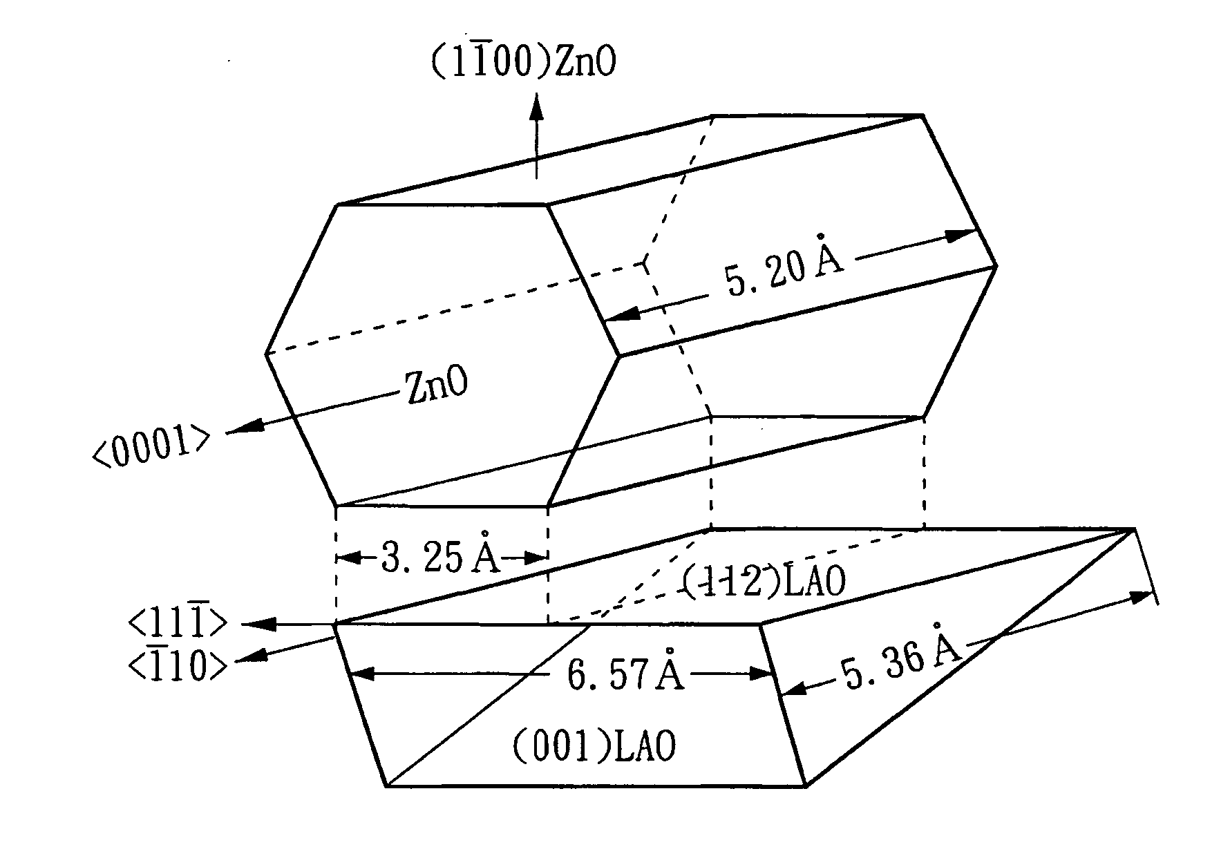
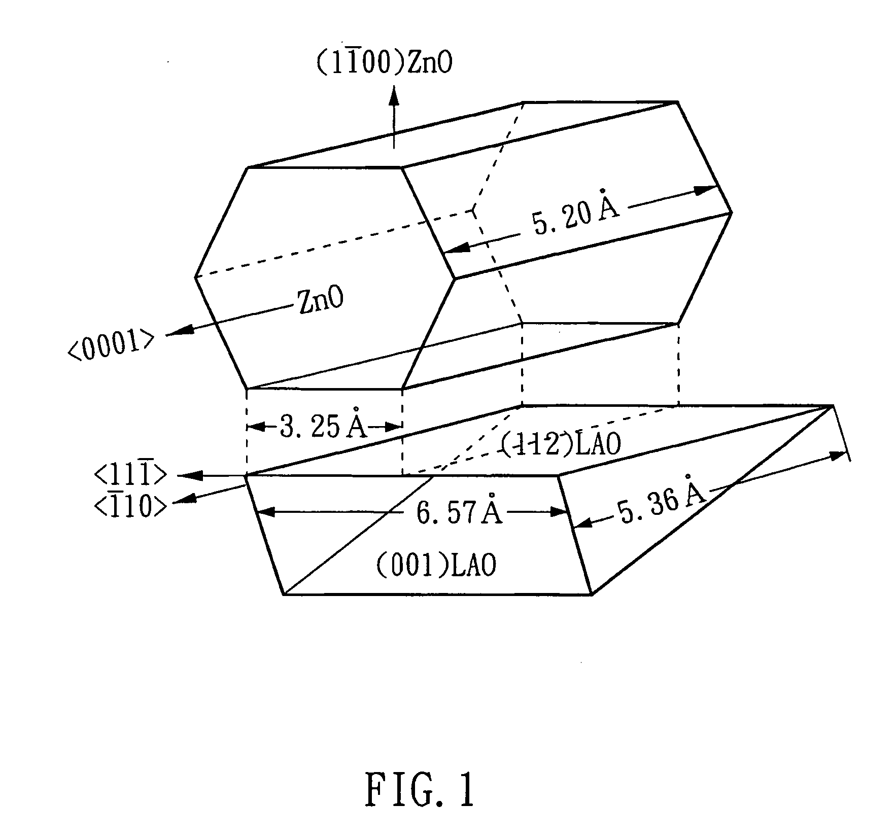
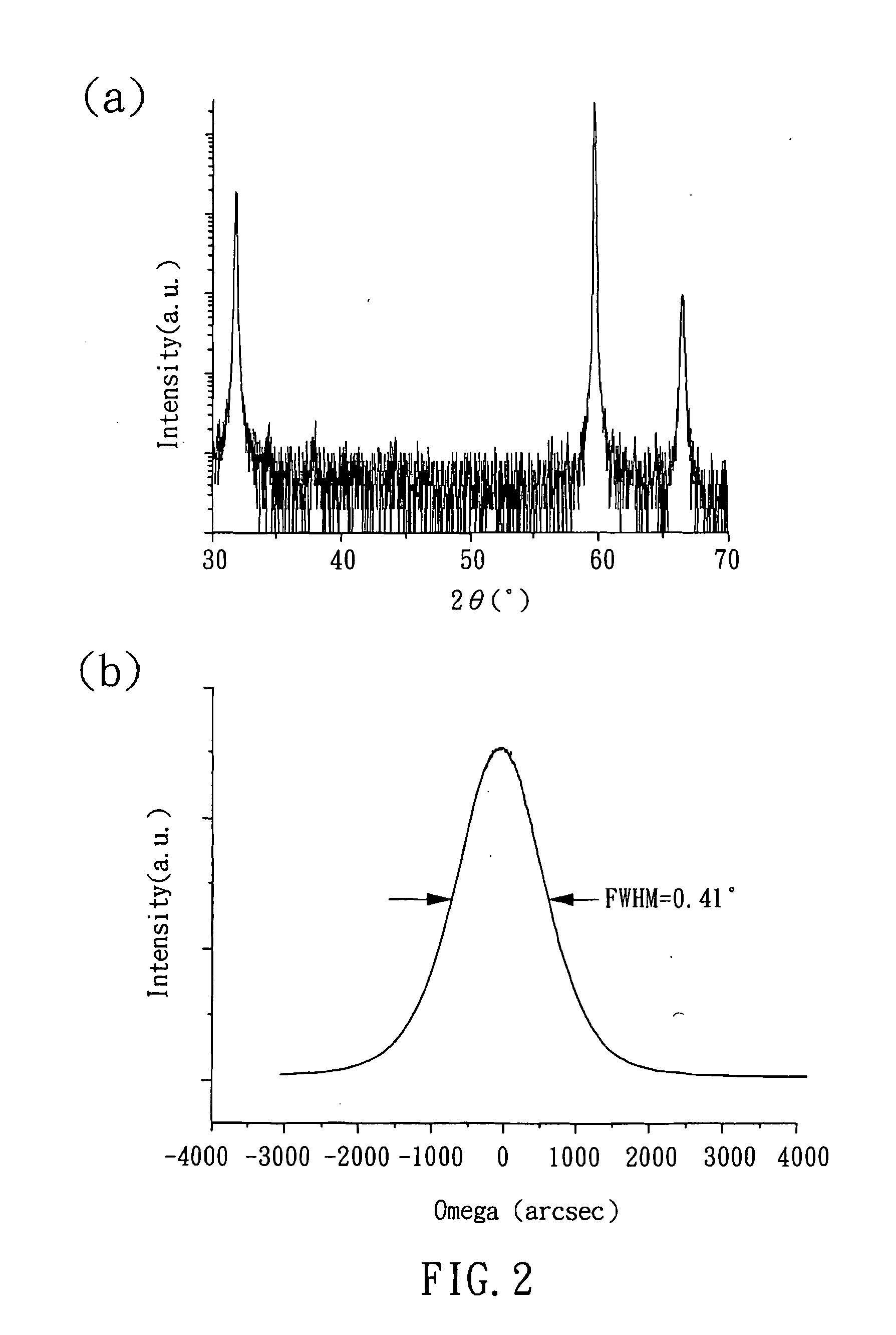
[0028]Then, a crystal plane or a cross section plane of the LaAlO3 single crystal oxide is used as a substrate, as shown in FIG. 1, which is a perspective view showing the growth of a non-polar m-plane epitaxial layer in the present embodiment. In the present embodiment, the plane with Miller index of {112} was used as a substrate. Then, the substrate was loaded into a chamber, washed with hot acetone and isopropanol...

embodiment 2

[0032]The materials and method used in the present embodiment are the same as those in Embodiment 1, except that the ablation target is a III-nitride, such as GaN which has similar lattice parameters (a=0.3189 nm, c=0.5185 nm) as ZnO. In the present embodiment, an epitaxial layer of III nitride, i.e. a GaN epitaxial layer, was obtained. The functions and the applications of the non-polar m-plane epitaxial layer of III nitride (GaN) grown in the present embodiment are the same as those of the epitaxial layer of ZnO grown in Embodiment 1.

[0033]Though only GaN was used as an ablation target in the present embodiment, other III-nitrides, such as indium nitride, aluminum nitride, indium gallium nitride, aluminum gallium nitride, aluminum indium nitride, aluminum indium gallium nitride, or a combination thereof, can also be used as an ablation target for growth of an epitaxial layer through the same method described in Embodiment 1. Also, the epitaxial layer formed by other III-nitrides h...

embodiment 3

[0034]The materials and method used in the present embodiment are the same as those in Embodiment 1 or 2, except that an oxide layer (not shown in the figure) was formed on the single crystal oxide, and a plane of the oxide layer was used as a substrate.

[0035]In the present embodiment, an SrTiO3 single crystal oxide with a perovskite structure was provided, and then an LaAIO3 oxide layer was formed on the SrTiO3 single crystal oxide. A plane of the LaAlO3 oxide layer with Miller Index of {112} was used as a substrate, and a non-polar m-plane epitaxial layer of wurtzite semiconductors was formed on the substrate through a vapor deposition process with the same deposition conditions as described in Embodiment 1. Though the SrTiO3 single crystal oxide and the LaAlO3 oxide layer were exemplified in the present embodiment, the compositions of the oxide layer and the single crystal oxide can be the same or different if it is needed. Also, the functions and applications of the epitaxial la...


PUM


Abstract

The present invention relates to a method for growing a non-polar m-plane epitaxial layer on a single crystal oxide substrate, which comprises the following steps: providing a single crystal oxide with a perovskite structure; using a plane of the single crystal oxide as a substrate; and forming an m-plane epitaxial layer of wurtzite semiconductors on the plane of the single crystal oxide by a vapor deposition process. The present invention also provides an epitaxial layer having an m-plane obtained according to the aforementioned method.

Description

BACKGROUND OF THE INVENTION[0001]1. Field of the Invention[0002]The present invention relates to a method for growing a non-polar m-plane epitaxial layer of wurtzite semiconductors on a single crystal oxide substrate and, more particularly, to a method for growing a non-polar m-plane epitaxial layer of ZnO or III-nitrides with the nature of both low lattice mismatch and good thermal stability. The present invention also provides an epitaxial layer having a non-polar m-plane obtained according to the aforementioned method.[0003]2. Description of Related Art[0004]Currently, GaN and other III-nitrides have attracted considerable interest for its successful applications on blue-to-UV light solid-state electronic devices and laser diodes. The crystal structures of these nitrides belong to a hexagonal wurtzite structure, so the crystals of these nitrides are grown along a c-axis direction [0001]. However, some studies found that a polarization effect along the c-axis may occur in c-axis G...

Claims


Application Information

Patent Timeline
IPC IPC(8): H01L29/22H01L21/34H01L21/20H01L29/20
CPCC30B23/025C30B25/18C30B29/16C30B29/403H01L29/2003H01L21/02538H01L21/02554H01L21/02609H01L29/04H01L21/0242
Inventor CHANG, LIHO, YEN-TENG
Owner NAT CHIAO TUNG UNIV
Why Eureka
Try Eureka