

Thin film transistor
- Summary
- Abstract
- Description
- Claims
- Application Information
AI Technical Summary
Benefits of technology
Problems solved by technology
Method used
Image

Examples
example 1
[0076]An example of producing the bottom-gate channel-protective oxide semiconductor TFT including the bilayer oxide semiconductor channel layer in FIG. 1 will be described.
[0077]First, the gate electrode 11 is formed on the glass substrate 10. As for the gate electrode 11, Mo is used as an electrode material and the film thickness is made 100 nm. After that, the gate electrode layer 11 is patterned by a photolithographic process and an etching process.
[0078]Next, a 200-nm silicon oxide layer is formed as the gate insulating layer 12 by a plasma CVD method. The substrate temperature upon the formation of the silicon oxide layer by the plasma CVD method is 340° C. Processing gases used are SiH4 and N2O and the proportion of the gas flow rates is SiH4:N2O=1:25. The supplied RF power density and the pressure are respectively 0.9 W / cm2 and 173 Pa.
[0079]An amorphous IGZO having a film thickness of 15 nm is formed as the first oxide semiconductor region (first region) 13. This oxide semic...
example 2
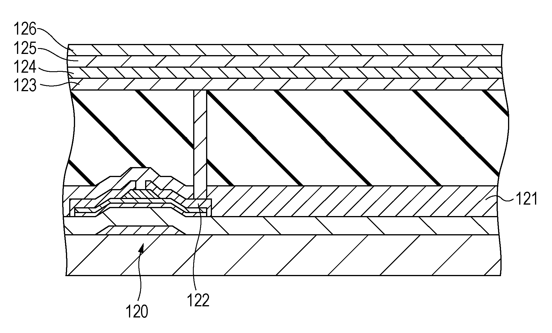
[0087]An example of producing the bottom-gate coplanar-structure oxide semiconductor TFT including a bilayer oxide semiconductor channel layer in FIG. 6 will be described.
[0088]As in EXAMPLE 1, the gate electrode 11, the gate insulating layer 12, the first oxide semiconductor channel layer 13, the second oxide semiconductor channel layer 14, and the channel protective layer 15 were formed on the glass substrate 10.
[0089]A silicon nitride layer having a film thickness of 300 nm was further formed as the protective layer 17 by a plasma CVD method. The substrate temperature upon the formation of the silicon nitride film by the plasma CVD method was 250° C. Processing gases used were SiH4, NH3, and N2 and the proportion of the gas flow rates was SiH4:NH3:N2=1:2.5:25. The supplied RF power density and the pressure were respectively 0.9 W / cm2 and 150 Pa. Simultaneously when the protective layer 17 was formed, the regions of the oxide semiconductor regions 13 and 14 without the channel pro...
example 3
[0104]An example of producing a top-gate coplanar-structure oxide semiconductor TFT including a bilayer oxide semiconductor channel layer in FIG. 11 will be described.
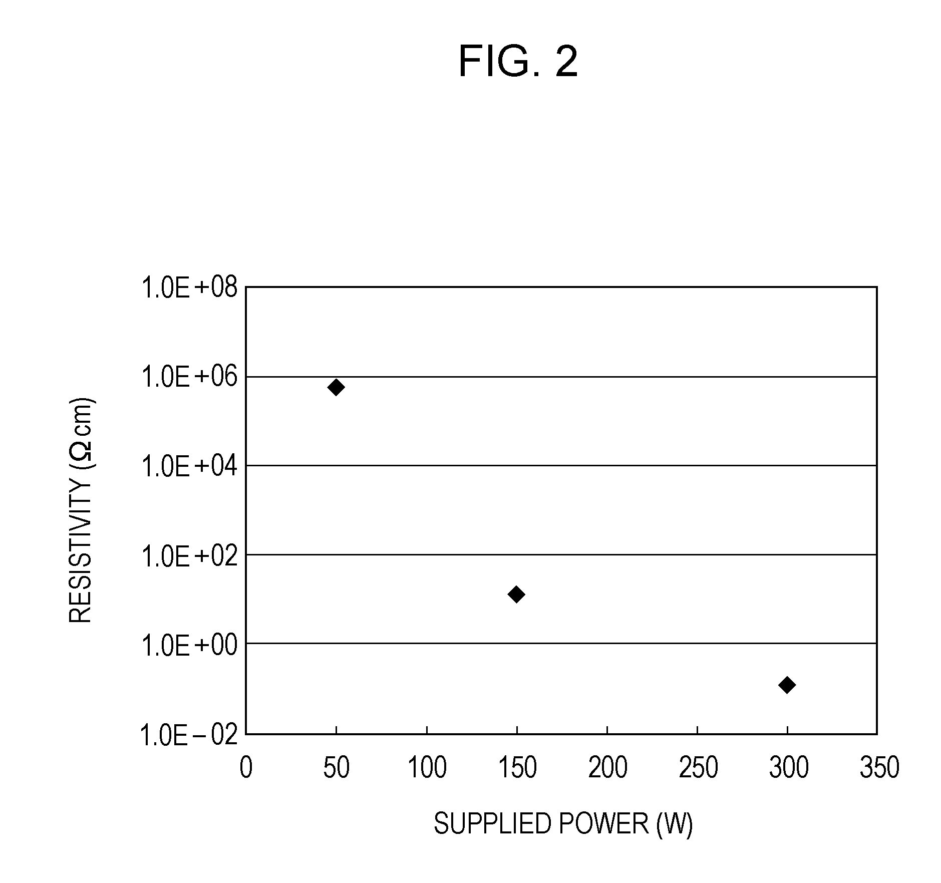
[0105]First, an amorphous IGZO having a film thickness of 15 nm is formed as the second oxide semiconductor channel layer 14 on the glass substrate 10. This oxide semiconductor layer is formed with a DC sputtering apparatus at a substrate temperature of room temperature (25° C.). The target used is a polycrystalline sinter having an InGaZnO4 composition and the supplied DC power is 50 W. The atmosphere upon the film formation is at a total pressure of 0.5 Pa and the gas flow rate at this time is Ar:O2=98:2.
[0106]Next, an amorphous IGZO having a film thickness of 15 nm is continuously formed as the first oxide semiconductor region 13. This oxide semiconductor layer is formed with a DC sputtering apparatus at a substrate temperature of room temperature (25° C.). The target used is a polycrystalline sinter having an InGaZ...
PUM
 Abstract
Description
Claims
Application Information