Curable polysiloxane composition, and polysiloxane cured product, optical member, member for aerospace industry, semiconductor light-emitting device, illuminating device and image display device using the same
a technology of polysiloxane and composition, which is applied in the direction of semiconductor devices, solid-state devices, basic electric elements, etc., can solve the problems of remarkable decrease in the luminance of the semiconductor light-emitting device, degradation of phosphor, etc., and achieves excellent heat resistance, light resistance, hydrothermal resistance, and uv resistance. , the effect of suppressing foaming
- Summary
- Abstract
- Description
- Claims
- Application Information
AI Technical Summary
Benefits of technology
Problems solved by technology
Method used
Image
Examples
embodiment a-1
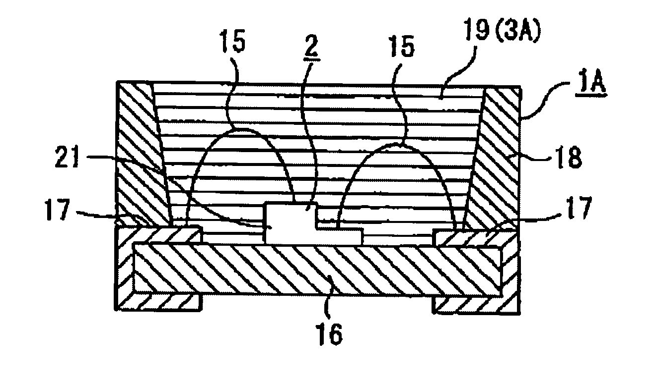
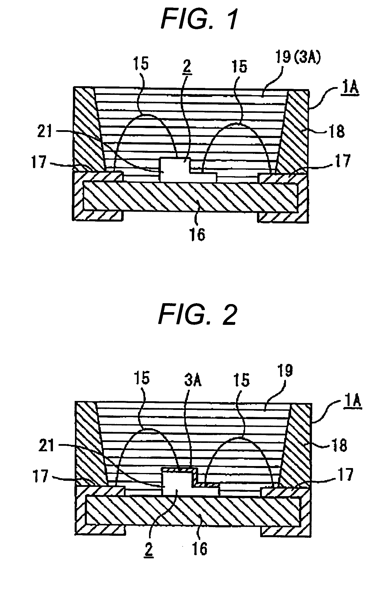
[0438]In light emitting device 1A of the present embodiment, as shown in FIG. 1, light-emitting element 2 is surface-mounted on an insulating substrate 16 on which printed wiring 17 is provided. In light-emitting element 2, a p-type semiconductor layer (not shown) and an n-type semiconductor layer (not shown) in light-emitting layer part 21 are each connected electrically to printed wirings 17 and 17 via conductive wires 15 and 15, respectively. Conductive wires 15 and 15 have a small cross sectional area so that the light emitted from light-emitting element 2 may not be interfered.
[0439]As light-emitting element 2, one that emits light of any wavelengths, from ultraviolet to infrared regions, may be used. In this embodiment, a gallium nitride-based LED chip is assumed to be used. In light-emitting element 2, an n-type semiconductor layer (not shown) is formed on the lower side in FIG. 1 and a p-type semiconductor layer (not shown) is formed on the upper side in FIG. 1. The upper si...
embodiment a-2
[0443]Light emitting device 1A of the present embodiment is constituted, as shown in FIG. 2, in the same manner as the above embodiment A-1, except that the front side of light-emitting element 2 is covered with transparent member 3A and the encapsulating part 19, formed on the transparent member, is formed of a material different from that of transparent member 3A. Transparent member 3A on the surface of light-emitting element 2 is a transparent thin film, functioning as a light extracting film and encapsulating film. Transparent member 3A can be formed, for example, by coating the above raw material of the polysiloxane cured product, by a method of spin coating or the like, during the formation of a chip of light-emitting element 2. Meanwhile, the same components as in the embodiment A-1 are designated by the same reference numerals to omit redundant explanations.
[0444]Thus, because light emitting device 1A of the present embodiment also comprises light-emitting element 2 and tran...
PUM
| Property | Measurement | Unit |
|---|---|---|
| Temperature | aaaaa | aaaaa |
| Temperature | aaaaa | aaaaa |
| Length | aaaaa | aaaaa |
Abstract
Description
Claims
Application Information


