
Laser drilling technique for creating nanoscale holes

a laser drilling and nano-sized technology, applied in the field of electrophysics and “ patch clamping, can solve the problems of multiple steps, slow approach, and difficult and/or time-consuming rie techniques for fabricating (micromachining) the pores in a quartz substra

Active Publication Date: 2011-05-12
WISCONSIN ALUMNI RES FOUND
View PDF4 Cites 21 Cited by
  • Summary
  • Abstract
  • Description
  • Claims
  • Application Information

AI Technical Summary

Benefits of technology

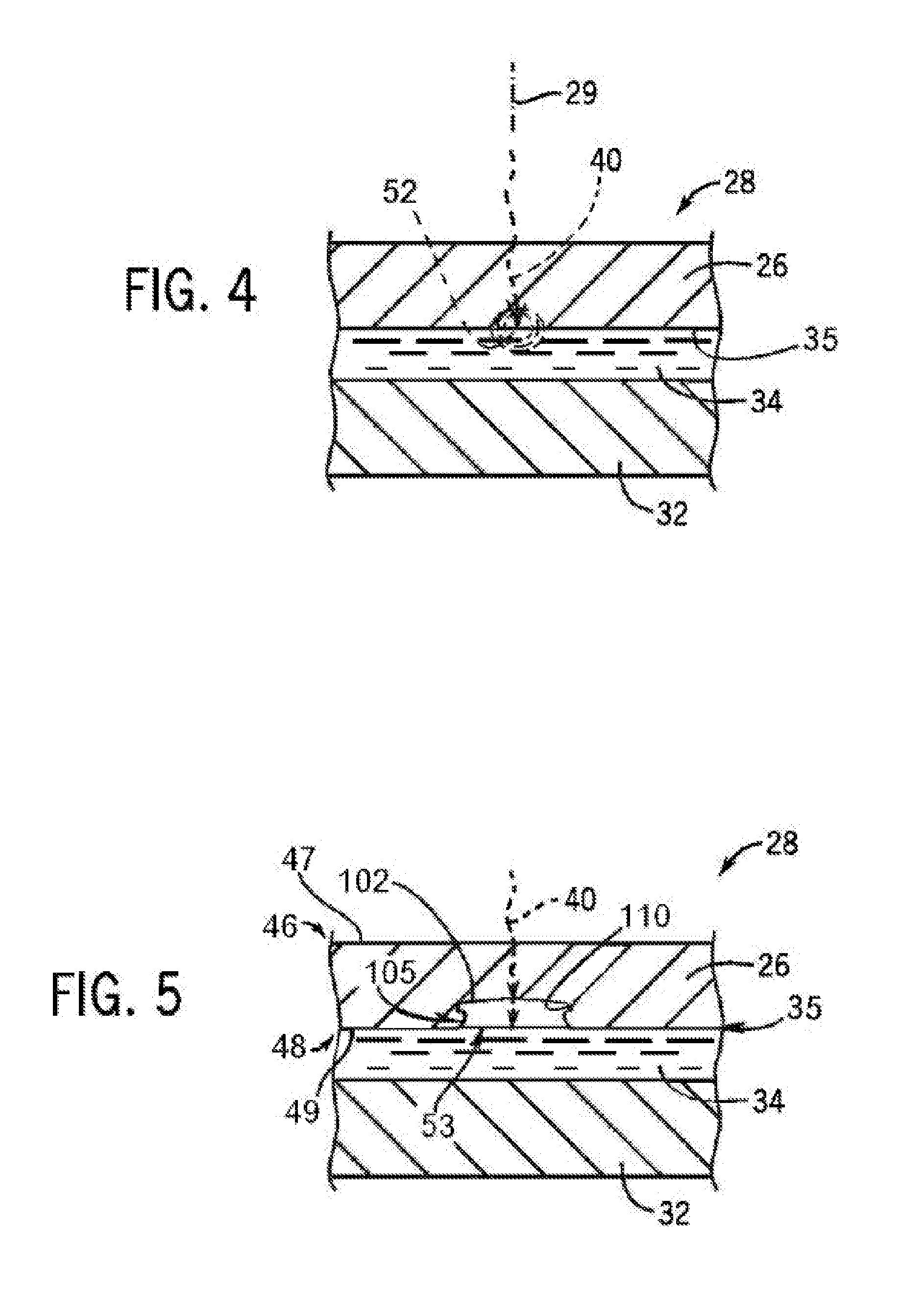
[0011]Specifically then, the present invention provides a method of creating nanoscale holes by using steps including creating a multi-layered assembly that comprises a substrate material and an energy absorbing material. The substrate material receives the nanoscale hole and defines a front side and an opposing back side. The energy absorbing material is adjacent the back side of the substrate material. A laser is applied through the multi-layered assembly, by initially passing through the substrate material and being focused at and absorbed by the energy absorbing material, increasing a temperature of the back side of the substrate material to a greater extent than an increase in temperature of the front side of the substrate material. Continued application of such laser stimulus to the energy absorbing material may correspondingly heat and / or pressurize the back side of the substrate, which can initiate a drilling of or establishing a pore through the substrate.
[0012]It is therefore an object of at least one embodiment of the invention to utilize a laser to drill a pore in a substrate by indirectly heating the substrate by focusing the laser at or near an interface between the substrate and an energy absorbing material. This allows for laser micromachining of a material that might otherwise be transparent to light of a wavelength emitted by the laser.
[0018]It is thus an object of at least one embodiment of the invention to provide a liquid medium for use as an energy absorbing material that can be placed under the substrate for performing a laser induce backside etching of the back side of the substrate. The backside etching may be performed on a quartz chip that has been pre-etched or thinned from an initially thick substrate. The initially thick substrate may be about 100-500 microns thick and can be either laser or wet etched, for example, with a buffered oxide etchant (BOE) or hydrofluoric (HF) etchant, in a pre-thinning procedure, down to about 20-50 microns in thickness before the nanopore laser drilling is initiated, which may improve suction and reduce series resistance.
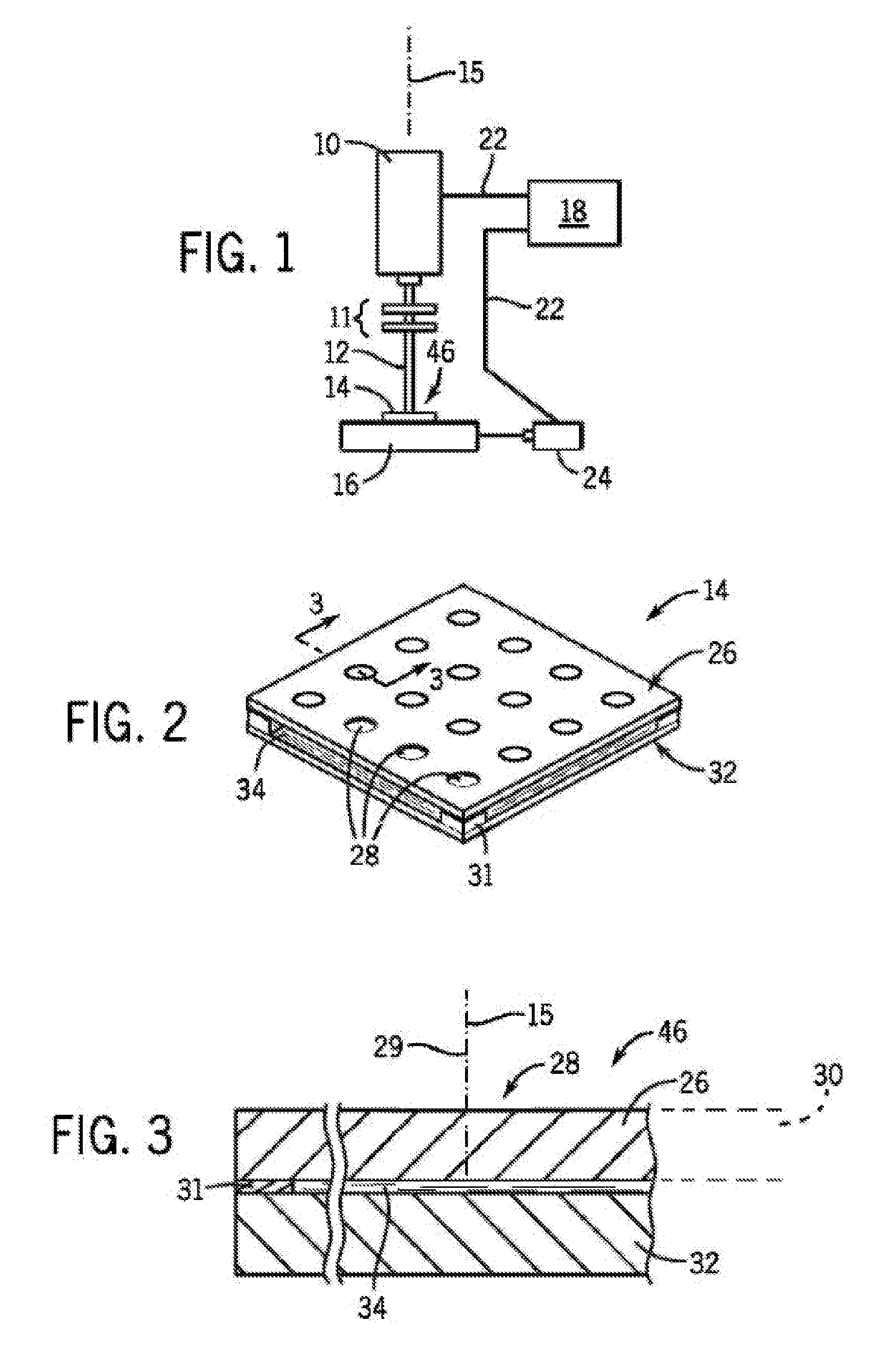
[0020]It is thus an object of at least one embodiment of the invention to provide a patch clamp chip that has a smooth pore that opens into a relatively larger diameter crater. This configuration can provide suitable structure to which a cell can be mounted.

Problems solved by technology

Despite a general recognition of quartz's suitability for use as a patch clamp substrate, many of its desirable characteristics, such as hardness, make fabricating (micromachining) the pores in a quartz substrate rather difficult and / or time consuming.
However, RIE techniques require multiple steps and are relatively slow processes.
However, since quartz has a wide band gap, this approach is also slow and is limited in terms of pore diameter and material thickness that can be achieved.
Since quartz is transparent to and therefore substantially unaffected by UV light(s), it has been widely accepted that excimer lasers are not usable for micromachining quartz.
Furthermore, although various patch clamping and other techniques have been developed and, at least to some extent, standardized for successfully modeling and investigating ion channel function voltage-sensitive (or voltage-gated) ion channels, in-depth investigation of yet other types of ion channels, such as mechanosensitive ion channels, remains at least somewhat frustrating and / or impracticable.

Method used


Image

  • Laser drilling technique for creating nanoscale holes
  • Laser drilling technique for creating nanoscale holes
  • Laser drilling technique for creating nanoscale holes

Examples


Embodiment Construction

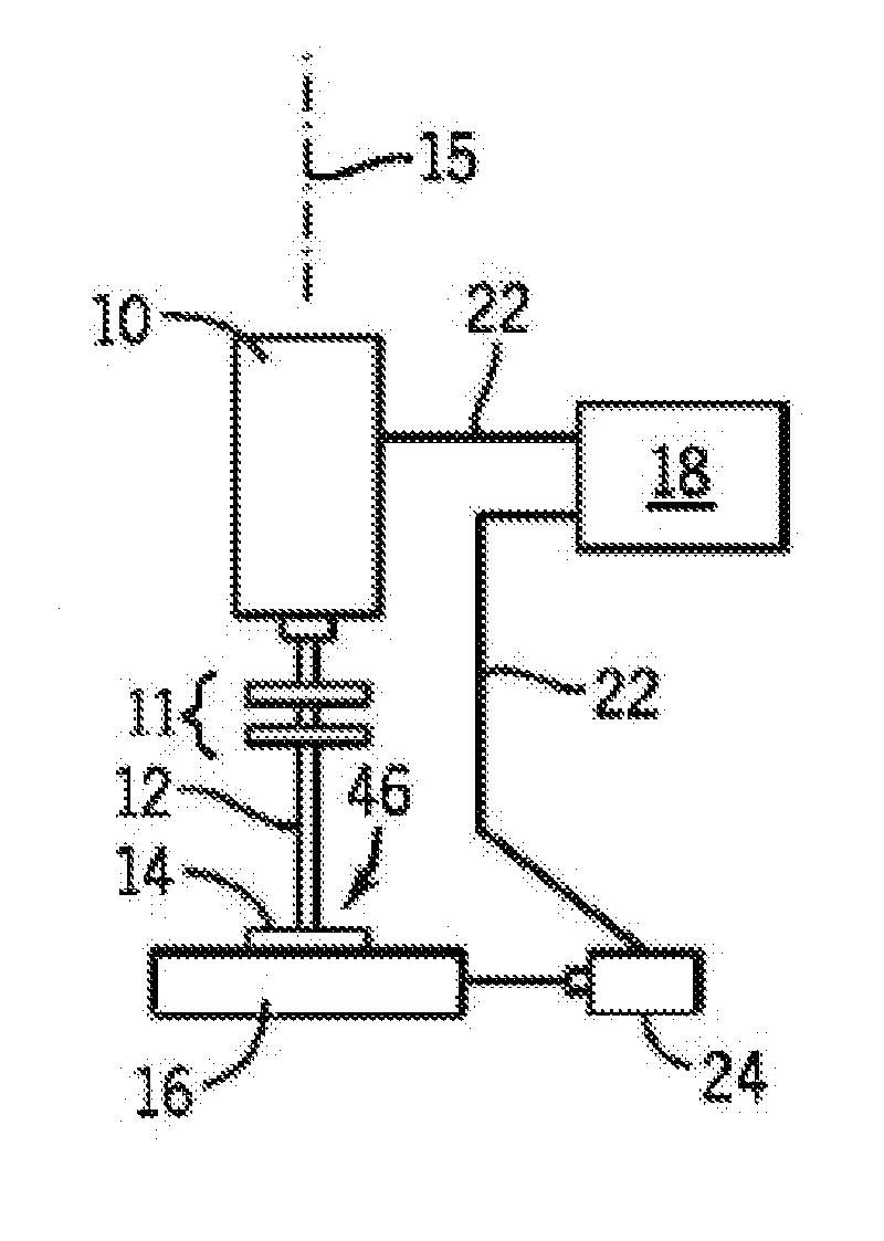
[0034]Referring now to FIG. 1, the present invention may use an ArF excimer laser 10 having collimating and focusing optics 11 to direct a narrow collimated beam 12 of light along an axis 15 toward a back surface of a sandwich-like, multi-layered assembly 14 that is held on a mechanical stage 16. The laser may, for example, have a wavelength range of about 155 nm to about 195 nm and is preferably operated to emit a beam 12 of light having a wavelength of about 193 nm. In other embodiments, laser 10 may be yet other types of lasers, such as CO2 lasers, and / or others, depending on, for example, a desired wavelength that is selected based on particular characteristics of components within the multi-layered assembly 14, in other words, how the multi-layered assembly 14 reacts to exposure to light having such wavelength(s), and / or other factors.

[0035]The laser 10 may include a variable attenuating mirror for controlling how much of the laser beam is to be transmitted, and a stencil metal...


PUM

PropertyMeasurementUnit
Fractionaaaaaaaaaa
Temperatureaaaaaaaaaa
Pore sizeaaaaaaaaaa

Abstract

A method of forming extremely small pores in a substrate that is used, for example, in patch clamp applications is provided that employs an energy absorbing material beyond a back side of the substrate to allow a laser to be focused adjacent the exit side of the substrate so as to generate a pore through the substrate and can also form a crater in the back side of the substrate and in which the pore may propagate from the crater in a drilling direction that can oppose a laser transmission direction.

Description

STATEMENT REGARDING FEDERALLY SPONSORED RESEARCH OR DEVELOPMENT[0001]N / A.CROSS REFERENCE TO RELATED APPLICATION[0002]N / A.BACKGROUND OF THE INVENTION[0003]The present invention relates to electrophysiology and “patch clamping” for investigating ionic and molecular transport through cellular membranes via ion channels and, in particular, to a substrate providing a set of nano to microscale pores that may be readily sealed to cellular membranes. Ion channel investigation using patch clamps often plays an important role in drug discovery and preliminary drug screening or evaluation, for example, by providing a model that shows an effect of a drug on ion channels. Doing so can be useful for either avoiding adverse effects or for creating a positive therapeutic effect for the treatment of ion channel related diseases.[0004]Drug screening can require a large number of ion channel measurements. Accordingly, in current practice, planar patch clamps are preferable because they allow paralleli...

Claims


Application Information

Patent Timeline
IPC IPC(8): B32B3/26B23K26/00
CPCY10T428/24281B23K26/18B23K26/4075B23K26/006Y10T428/24612G01N27/00B23K26/0656B23K26/381Y10T428/24273B23K26/382B23K26/066B23K26/40B23K26/55B23K2103/50
Inventor BLICK, ROBERT H.YU, MINRUI
Owner WISCONSIN ALUMNI RES FOUND
Learn More