Organic el device

a technology of organic el and el-type, applied in the direction of organic semiconductor devices, thermoelectric devices, solid-state devices, etc., can solve the problems of increased drive voltage, reduced production yield of display panels, and device defects, and achieve excellent hole injection capacity and electron transport capacity, high electron mobility, and the effect of increasing the thickness of the layer

Active Publication Date: 2011-06-16
SHARP KK
View PDF8 Cites 11 Cited by
  • Summary
  • Abstract
  • Description
  • Claims
  • Application Information

AI Technical Summary

Benefits of technology

[0026]In the configuration in accordance with the present invention, the hole injection layer is constituted by a host material formed of an n-type semiconductor material and a guest material formed of a p-type semiconductor, and because the p-type semiconductor functions as an n-type dopant in the host material, it is possible to obtain a hole injection layer having excellent hole injection capacity and electron transport capacity. The hole injection layer in accordance with the present invention has high electron mobility. Therefore, the layer thickness can be increased, without raising the device drive voltage. The increase in film thickness suppresses the occurrence of defects caused by particles present on the substrate, increases productivity, and makes it possible to produce organic EL devices with a high yield. Further, since the degree of freedom in designing the film thickness is increased, it is possible to design an organic EL layer with consideration for optical interference, without sacrificing the hole-electron balance in the light-emitting layer and drive voltage. In addition, the excellent hole injection capacity and hole transport capacity of the hole injection layer provide an organic EL device with a low drive voltage and long service life.

Problems solved by technology

However, when the thickness of the entire layer is reduced, it can easily induce device defects by a short circuit between the positive electrode and negative electrode caused by particles that have adhered to the substrate.
In particular, a large number of pixel defects and / or line defects appear in a flat panel display and the production yield of display panel decreases significantly.
Therefore, from the standpoint of increasing the production yield, it is preferred that the thickness of the entire organic EL device be large, but this results in increased drive voltage.
Thus, there is a tradeoff between a problem of reducing the drive voltage and a problem of increasing the yield.
When the effective mobility of carriers is increased and the driving voltage is decreased by doping a carrier transport layer with a dopant, as with the conventional technique, the following problem is encountered.
However, these materials have low stability in the air and require attention in handling.
In addition, in most cases, an expensive vapor deposition source is required.
Furthermore, because of their small atomic radii (subnanometer order), alkali metals easily migrate in the organic EL layer and can contaminate other layers constituting the organic EL layer.
A problem associated with the configuration using the n-type semiconductor as the hole injection layer is that the electron mobility of the n-type semiconductor is not necessarily high.
Further, a reflection component at the interface occurring when light is emitted from the device is especially large in an organic EL device using a low-molecular material.
In addition, the emission spectrum and emission luminance of the organic EL device are strongly affected by multiple interference of light in the device.
However, it is somewhat difficult to design the thickness of each layer with consideration for the effect produced on the drive voltage and the balance of holes and electrons inside the light-emitting layer.

Method used


Image

  • Organic el device
  • Organic el device
  • Organic el device

Examples


reference example 1

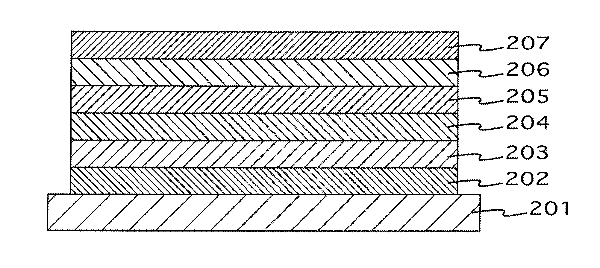
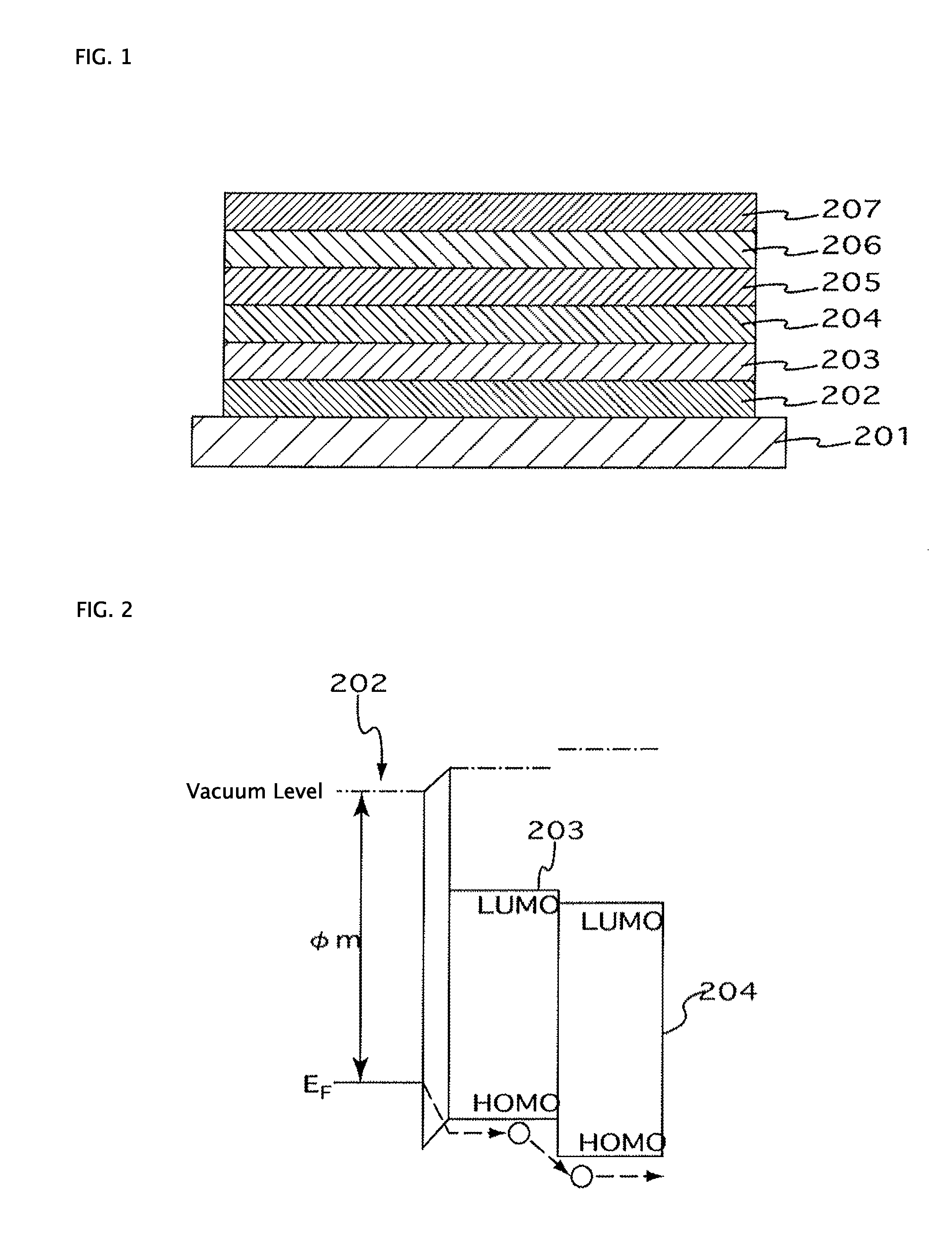
[0101]The object of the present reference example is to verify the height of carrier mobility in the hole injection layer used in the organic EL device in accordance with the present invention. An IZO film with a thickness of 110 nm was formed on a glass substrate (length 50 mm×width 50 mm×thickness 0.7 mm; Corning 1737 glass) by using a DC magnetron sputtering method (target: In2O3+10 wt. % ZnO, discharge gas: Ar+0.5 vol. % O2, discharge pressure: 0.3 Pa, discharge power: 1.45 W / cm2, substrate conveying rate 162 mm / min). An IZO electrode was then formed by processing the obtained IZO film by photolithography to a stripe shape with a width of 2 mm.

[0102]An NPB-doped HAT-6CN film with a thickness of 100 nm was then formed by resistance heating vapor deposition of HAT-6CN (Ip≈5.8 eV) and NPB (Ip=5.4 eV) simultaneously on the IZO electrode. In this case, the vapor deposition rate of HAT-6CN was set to 1 Å / s and the vapor deposition rate of NPB was set to 0.25 Å / s. The content of NPB in...

reference example 2

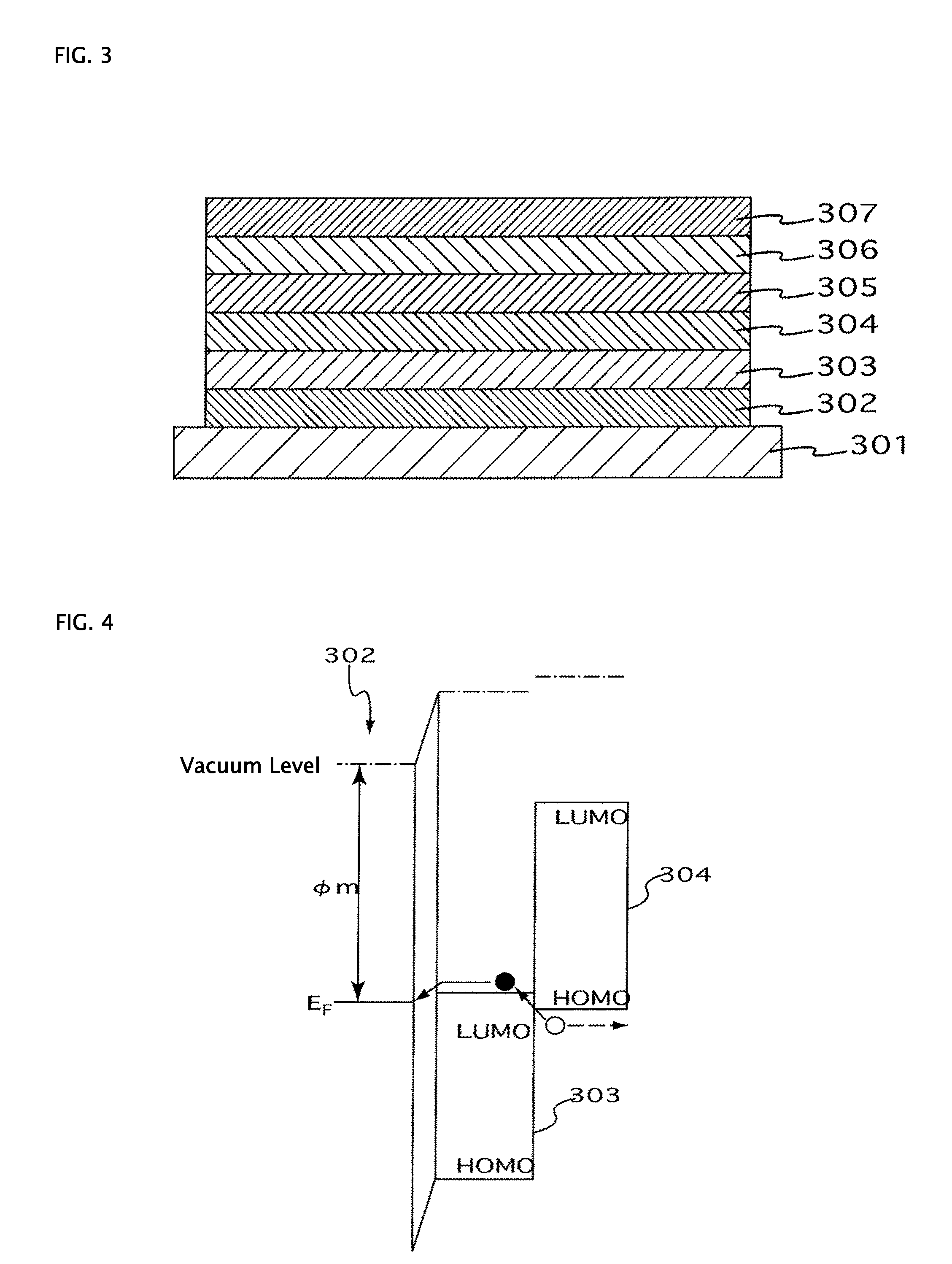
[0104]A model device was obtained by repeating the procedure of Reference Example 1, except that the NPB deposition rate was set to 1.75 Å / s. The content of NPB in the obtained NPB-doped HAT-6CN film calculated from a film thickness ratio was about 45 mol % based on the total number of molecules in the film.

example 1

[0108]Corning 1737 glass (length 50 mm×width 50 mm×thickness 0.7 mm) was used as the substrate 101. An IZO film with a thickness of 110 nm was formed on the substrate 101 by using a DC magnetron sputtering method (target: In2O3+10 wt. % ZnO, discharge gas: Ar+0.5 vol. % O2, discharge pressure: 0.3 Pa, discharge power: 1.45 W / cm2, substrate conveying rate 162 mm / min). A positive electrode 102 with a film thickness of 110 nm and a width of 2 mm was then formed by processing the obtained IZO film by photolithography to a stripe shape with a width of 2 mm.

[0109]A hole injection layer 103 composed of a NPB-doped HAT-6CN film with a thickness of 200 nm was then formed on the positive electrode 102 by resistance heating vapor deposition of HAT-6CN and NPB simultaneously. In this case, the deposition rate of HAT-6CN was set to 1 Å / s and the deposition rate of NPB was set to 0.9 Å / s. The content of NPB in the obtained hole injection layer 103 calculated from a volume ratio was about 30 mol %...


PUM


Abstract

The object of the present invention is to provide an organic EL device having a structure that resolves a problem of trade-off between decrease in a drive voltage and increase in production yield. The organic EL device of the present invention includes a substrate, a pair of electrodes provided on the substrate, and an organic EL layer sandwiched by the pair of electrodes; the pair of electrodes includes a positive electrode and a negative electrode; the organic EL layer includes at least a light-emitting layer and a hole injection layer that is in contact with the positive electrode; the hole injection layer is formed of an n-type semiconductor host material and a p-type semiconductor guest material; a LUMO level EHIC of the host material and a HOMO level of the guest material or a valence band level EGV satisfy:
|EHIC|+0.5 eV≧|EGV|>IHIC|−0.6 eV.

Description

TECHNICAL FIELD[0001]The present invention relates to an organic EL device that can be applied to flat panel displays and light sources for illumination. In particular, it is an object of the present invention to provide an organic electroluminescence device that operates at a low drive voltage and has low power consumption.BACKGROUND ART[0002]Organic electroluminescence devices (referred to hereinbelow as organic EL devices) have been actively researched in recent years with the object of putting them to practical use. Organic EL devices can realize a high current density at a low voltage and are therefore expected to realize high emission luminance and emission efficiency. The organic EL device is provided with a first electrode and a second electrode that sandwich an organic EL layer, and the electrode on the light take-out side is required to have high transmittance transparent conductive oxide film (TCO) materials (for example, indium tin oxide (ITO), indium zinc oxide (IZO), a...

Claims


Application Information

Patent Timeline
Patent Type & Authority Applications(United States)
IPC IPC(8): H01L51/54
CPCH01L51/0072H01L2251/552H01L51/5088H10K85/6572H10K50/17H10K2101/30
Inventor TERAO, YUTAKA
Owner SHARP KK
Why Eureka
Try Eureka