
Sub-wavelength structure layer, method for fabricating the same and photoelectric conversion device applying the same

a technology of structure layer and photolithography process, which is applied in the direction of solid-state devices, semiconductor devices, electrical devices, etc., can solve the problems of high manufacturing cost, limited application, and high cost of sub-wavelength anti-reflective structure fabricated by expensive and complex photolithography process, etc., to achieve excellent anti-reflection effect, enhance light output power, and simple and low cost technology

Inactive Publication Date: 2011-06-23
NAT CHIAO TUNG UNIV
View PDF12 Cites 18 Cited by
  • Summary
  • Abstract
  • Description
  • Claims
  • Application Information

AI Technical Summary

Benefits of technology

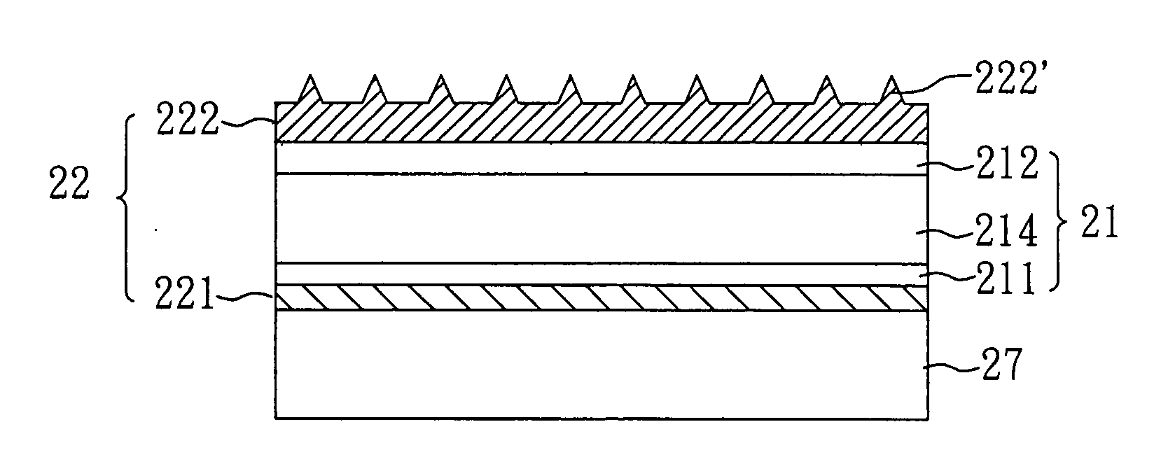
[0010]The object of the present invention is to provide a method for fabricating a sub-wavelength structure layer, where a sub-wavelength structure is fabricated by a simple and low cost technology to obtain an antireflective layer with an excellent antireflection effect. Also, the inventors provide an idea that the above-mentioned method for fabricating a sub-wavelength structure can be applied to texturing the surface of an n-GaN layer for thin GaN flip chip LED process to enhance the light output power and for vertical LED (thin GaN) process, and can be applied to texturing the surface of an transparent conductive oxide layer (TCO layer) to enhance light trapping of a thin-film solar cell or the like.
[0012]Accordingly, in the present invention, a sub-wavelength structure is fabricated through self-assembly of metal upon being heated. In comparison to a conventional photolithography process, the present invention has advantages in low cost and simple process. Additionally, the passivation layer with the sub-wavelength structure on a surface thereof according to the present invention can be used as an antireflection layer and exhibits a better antireflection effect than a film-shaped antireflective layer fabricated by a conventional coating process. Besides, the n-GaN layer with the sub-wavelength structure on a surface thereof can enhance light output in the case of being applied in an LED device or the like, while the transparent conductive oxide layer with the sub-wavelength structure on a surface thereof can enhance light trapping and thus improve light absorption in the case of being applied in a thin-film solar cell or the like. Moreover, in comparison to a conventional process where the sub-wavelength structure is fabricated on the surface of the silicon substrate and then coated with a passivation layer, the present invention can omit the problem of non-uniform coating of a passivation layer on the sub-wavelength structure by fabricating a sub-wavelength structure on a passivation layer. Meanwhile, in the case of fabricating a sub-wavelength structure on a passivation layer according to the present invention, the possibility of the semiconductor layer being damaged by reactive ion etching can be reduced, resulting in improved conversion efficiency of a photoelectric conversion device.
[0017]Accordingly, the present invention further provides a sub-wavelength structure layer, which is a passivation layer, an n-GaN layer or a transparent conductive oxide layer of which a surface has a sub-wavelength structure, where the sub-wavelength structure has a height of from 150 nm to 160 nm, and the cross-sectional area of the sub-wavelength structure increases along the thickness direction of the passivation layer, the n-GaN layer or the transparent conductive oxide layer. Herein, the passivation layer with the sub-wavelength structure may have a reflectivity of 10% or less over a wavelength from 400 nm to 700 nm and a reflectivity of 1% or less over a wavelength from 582 nm to 680 nm. Thereby, the passivation layer with a sub-wavelength structure provided by the present invention exhibits improved antireflection effect, and thus can enhance the amount of light extraction when being applied in a photoelectric conversion device as an antireflective layer to obtain a photoelectric conversion device with high efficiency, such as a solar cell. In addition, the n-GaN layer with a sub-wavelength structure provided by the present invention can be applied in LEDs or the like to enhance light output of LEDs or the like. Moreover, the transparent conductive oxide layer with the sub-wavelength structure can be applied in a thin-film solar cell or the like to enhance light trapping and thus improve light absorption.

Problems solved by technology

Although the use of the antireflective layer with a multi-layer structure can efficiently reduce the reflection of the incident light, the manufacturing cost therefore is higher and its application is restricted due to thermal mismatch and thermal diffusion.
Mainly, the sub-wavelength antireflective structure is fabricated by an expensive and complex photolithography process.
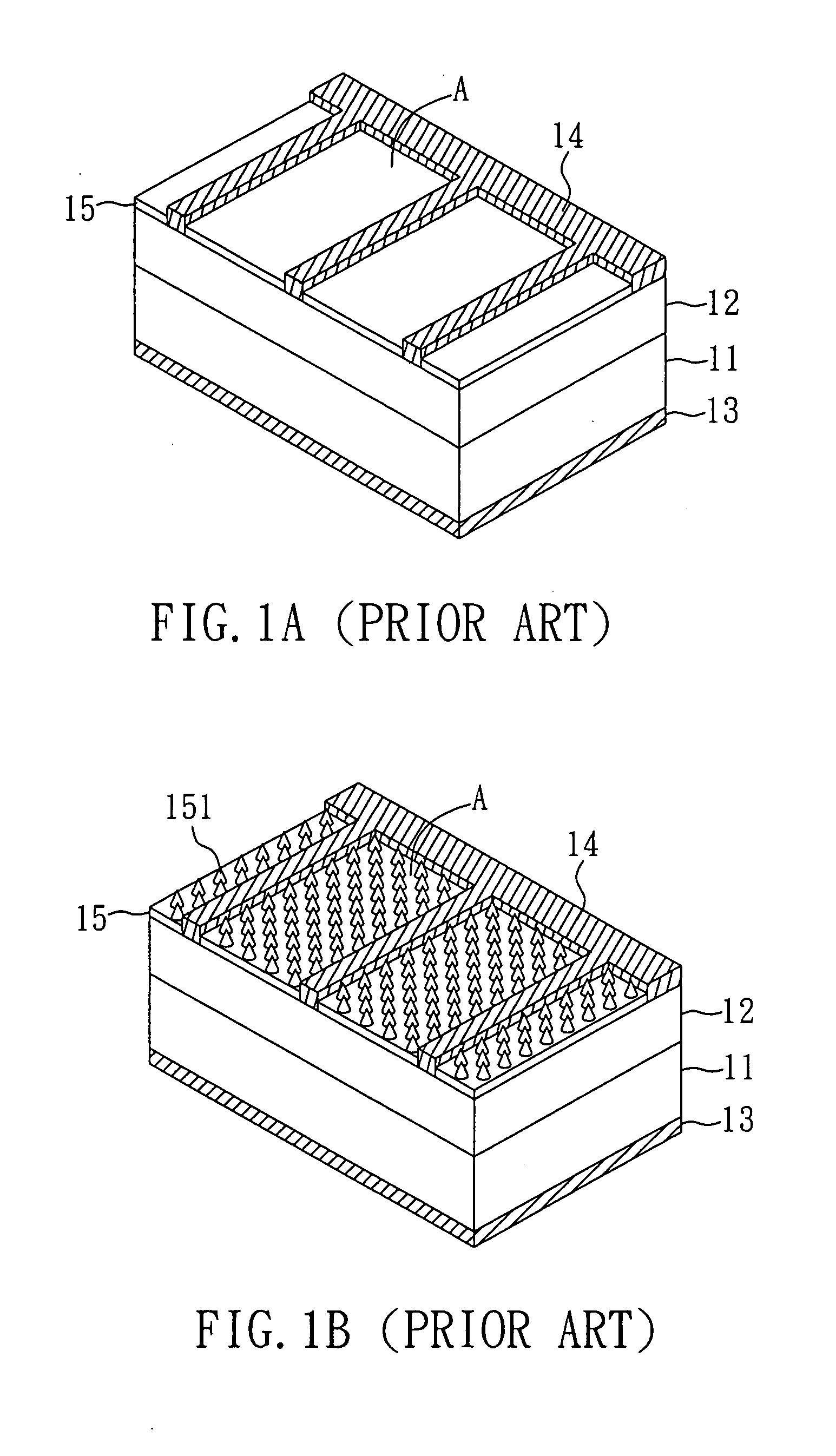
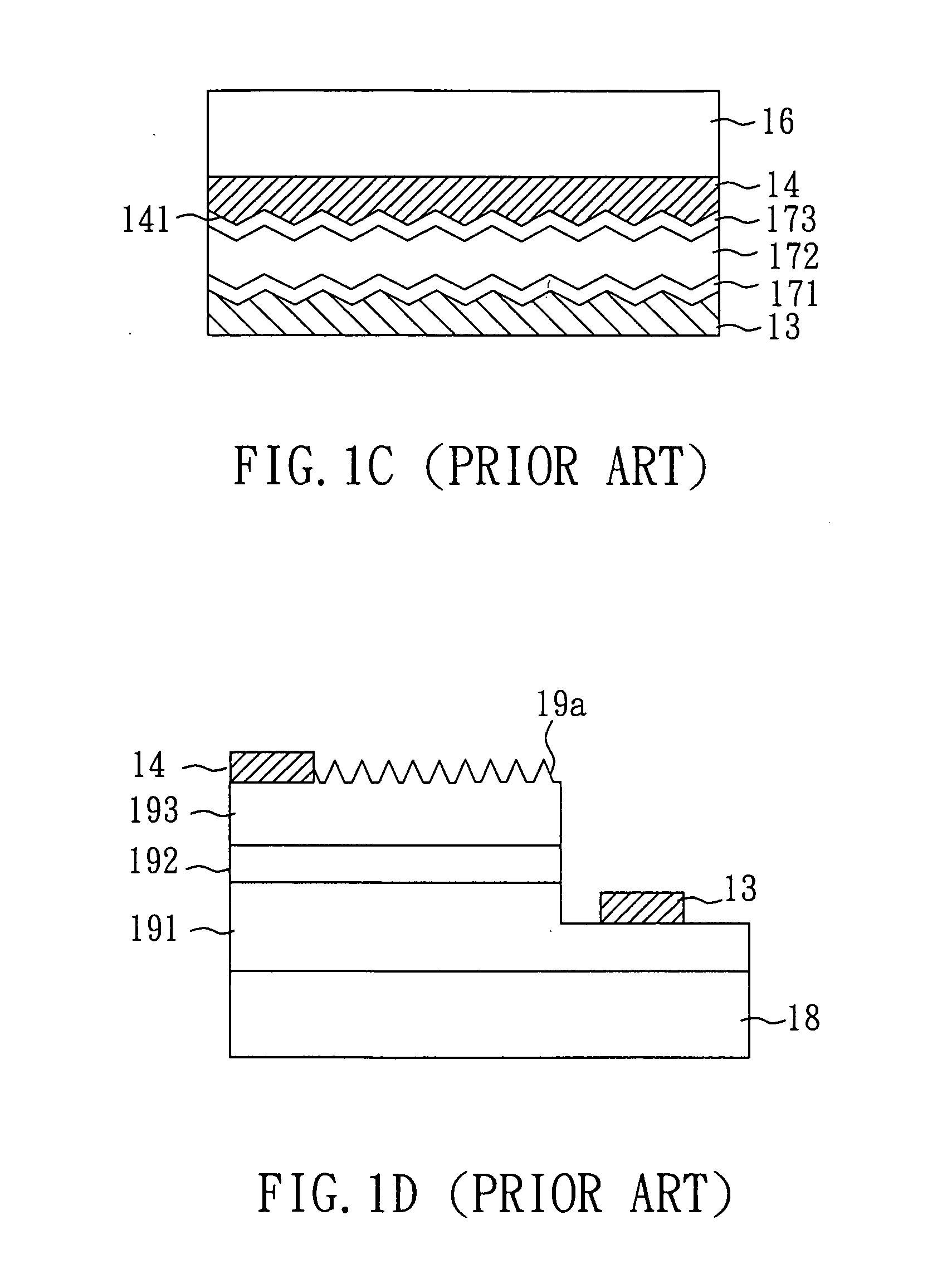
In addition to solar cells, surface texture is also an important issue for LEDs (light-emitting diodes).
In general, texturization on the surface of the p-GaN layer 193 is performed by dry or wet etching, where an expensive and complex lithography process is required to define the pattern in dry etching.

Method used


Image

  • Sub-wavelength structure layer, method for fabricating the same and photoelectric conversion device applying the same
  • Sub-wavelength structure layer, method for fabricating the same and photoelectric conversion device applying the same
  • Sub-wavelength structure layer, method for fabricating the same and photoelectric conversion device applying the same

Examples


example 1

[0042]FIGS. 2A to 2E show a process for fabricating a sub-wavelength structure layer as an antireflective layer on a silicon wafer.

[0043]First, as shown in FIG. 2A, a (100) silicon wafer 20 was cleaned with diluted HF to remove the native oxide. Subsequently, a 200±5 nm thick passivation layer 25 was deposited on the silicon wafer 20 by plasma enhanced chemical vapor deposition (PECVD) technique. In the present example, the passivation layer 25 was a silicon nitride (Si3N4) layer.

[0044]Next, as shown in FIG. 2B, a metal film 26 with a thickness of 15±0.5 nm was evaporated on the surface of the passivation layer 25 using an E-beam evaporating system. In the present example, the metal film 26 was made of nickel.

[0045]As shown in FIG. 2C, the metal film was then rapid-thermally annealed under the gas mixture of H2 and N2 with a flow rate of 3 sccm at 850° C. for 60 seconds to form self-assembled metal nano particles 26′ (owing to surface tension), which served as a mask for the passiva...

example 2

[0048]The fabricating process was the same as that illustrated in the Example 1, except that the metal film was made of gold and the metal nano particles were removed using an etchant composed of potassium iodide and iodine. In the present example, the heat treatment was performed on the metal film at 850° C. for 60 seconds.

experimental example

[0050]The sample of Example 1 was compared to those of Comparative Examples 1 to 3 in reflectivity, and the result is shown in FIG. 3. As shown in FIG. 3, the untreated blank silicon wafer (Comparative Example 1) exhibits high reflection >35% for visible and near infrared wavelengths; the single-layer antireflective layer of silicon nitride (Comparative Example 2) exhibits low reflection 35% for shorter wavelength 400 nm; and the two-layer antireflective layer of silicon nitride / magnesium fluoride (Comparative Example 3) exhibits low reflection 20% for shorter wavelength 400 nm, while the sub-wavelength structure of silicon nitride (Example 1) shows reflection <10% for wavelengths from 400 nm to 700 nm and reduced reflection <1% for wavelengths from 580 nm to 680 nm.

[0051]Thereby, it can be confirmed that the antireflective layer according to the present invention exhibits an excellent antireflection effect, and thus can enhance the amount of light extraction when being applied in a...


PUM

PropertyMeasurementUnit
thicknessaaaaaaaaaa
diameteraaaaaaaaaa
heightaaaaaaaaaa

Abstract

The present invention relates to a method for fabricating a sub-wavelength structure layer, including: forming a metal film on a passivation layer, an n-GaN layer or a transparent conductive oxide layer; performing thermal treatment to form self assembled metal nano particles; using the metal nano particles as a mask to remove a partial area of the passivation layer, the n-GaN layer or the transparent conductive oxide layer to form a sub-wavelength structure of which the cross-sectional area increases along the thickness direction of the passivation layer, the n-GaN layer or the transparent conductive oxide layer; and removing the metal nano particles. In addition, the present invention further provides the obtained sub-wavelength structure layer and a photoelectric conversion device using the same.

Description

BACKGROUND OF THE INVENTION [0001]1. Field of the Invention[0002]The present invention relates to a sub-wavelength structure layer and its manufacturing method and application and, more particularly, to a sub-wavelength structure layer suitable for a photoelectric conversion device and its manufacturing method and application.[0003]2. Description of Related Art[0004]Antireflective layers can be applied in various products, and more particularly, in the solar energy industry that has developed rapidly in recent years. The solar cell is a photoelectric conversion device to convert light into electricity. The most common known solar cell is configured as a p-n junction, which is formed by joining p-type and n-type semiconductors together in very close contact. After the p-n junction absorbs light and separates electrons and holes, the electric field opposes the obtained electrons and holes moving to the n-type and p-type semiconductors respectively to contribute current. Finally, the c...

Claims


Application Information

Patent Timeline
Patent Type & Authority Applications(United States)
IPC IPC(8): H01L31/0224H01L31/18H01L31/0352
CPCH01L31/02168Y02E10/50H01L33/22H01L31/0236
Inventor CHANG, EDWARD YISAHOO, KARTIKA CHANDRALIN, MEN-KULU, YI-YAOWANG, SHENG-PING
Owner NAT CHIAO TUNG UNIV
Learn More