Liquid crystal display device and electronic device

a liquid crystal display device and electronic device technology, applied in static indicating devices, instruments, non-linear optics, etc., can solve the problems of increasing increasing the operation temperature, and difficult for liquid crystal display devices, so as to reduce the amount of leakage of image signals through transistors, suppress display degradation (reduction of display quality), and reduce power consumption of liquid crystal display devices

Active Publication Date: 2011-06-23
SEMICON ENERGY LAB CO LTD
View PDF102 Cites 49 Cited by
  • Summary
  • Abstract
  • Description
  • Claims
  • Application Information

AI Technical Summary

Benefits of technology

[0013]In a liquid crystal display device which is an embodiment of the present invention, a transistor whose channel formation region is formed using an oxide semiconductor layer is used as the transistor provided in each pixel. Note that with the use of the high-purity oxide semiconductor layer, off-state current of the transistor at a room temperature can be 10 aA/μm or less and off-state current at 85° C. can be 100 aA/μm or less. Therefore, the amount of leakage of an image signal through the transistor can be reduced. That is, display degradation (change) which occurs when writing frequency of an image signal to a pixel included in the transistor is reduced can be suppressed. Thus, power consumption of the liquid crystal display device can be reduced and display degradation (reduction in display qual...

Problems solved by technology

Specifically, the amount of leakage of an image signal through the transistor is increased along with increase in the operation temperature.
Therefore, it is difficu...

Method used


Image

  • Liquid crystal display device and electronic device
  • Liquid crystal display device and electronic device
  • Liquid crystal display device and electronic device

Examples


embodiment 1

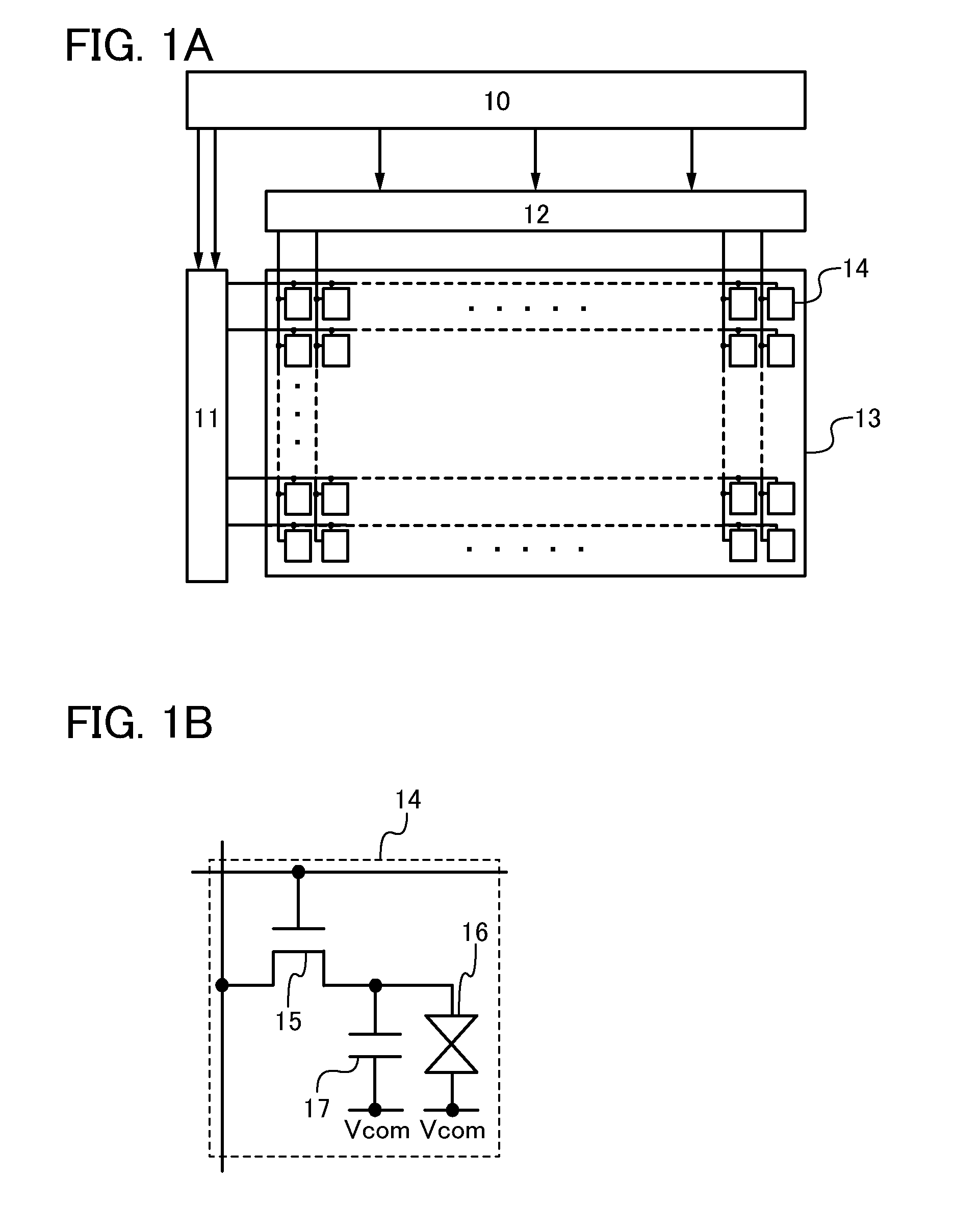
[0027]In this embodiment, an example of an active matrix liquid crystal display device is described. Specifically, an active matrix liquid crystal display device which can select input of an image signal to a pixel portion is described with reference to FIGS. 1A and 1B, FIG. 2, and FIGS. 3A to 3C.

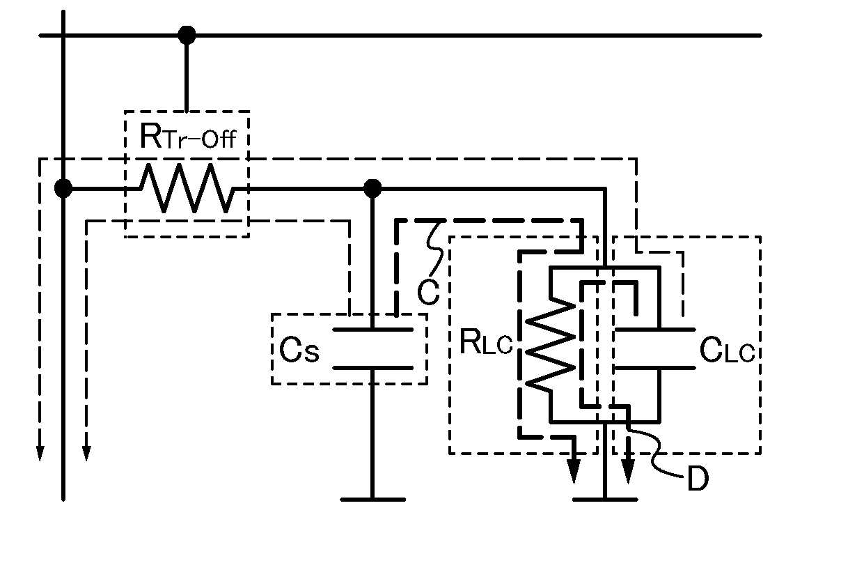
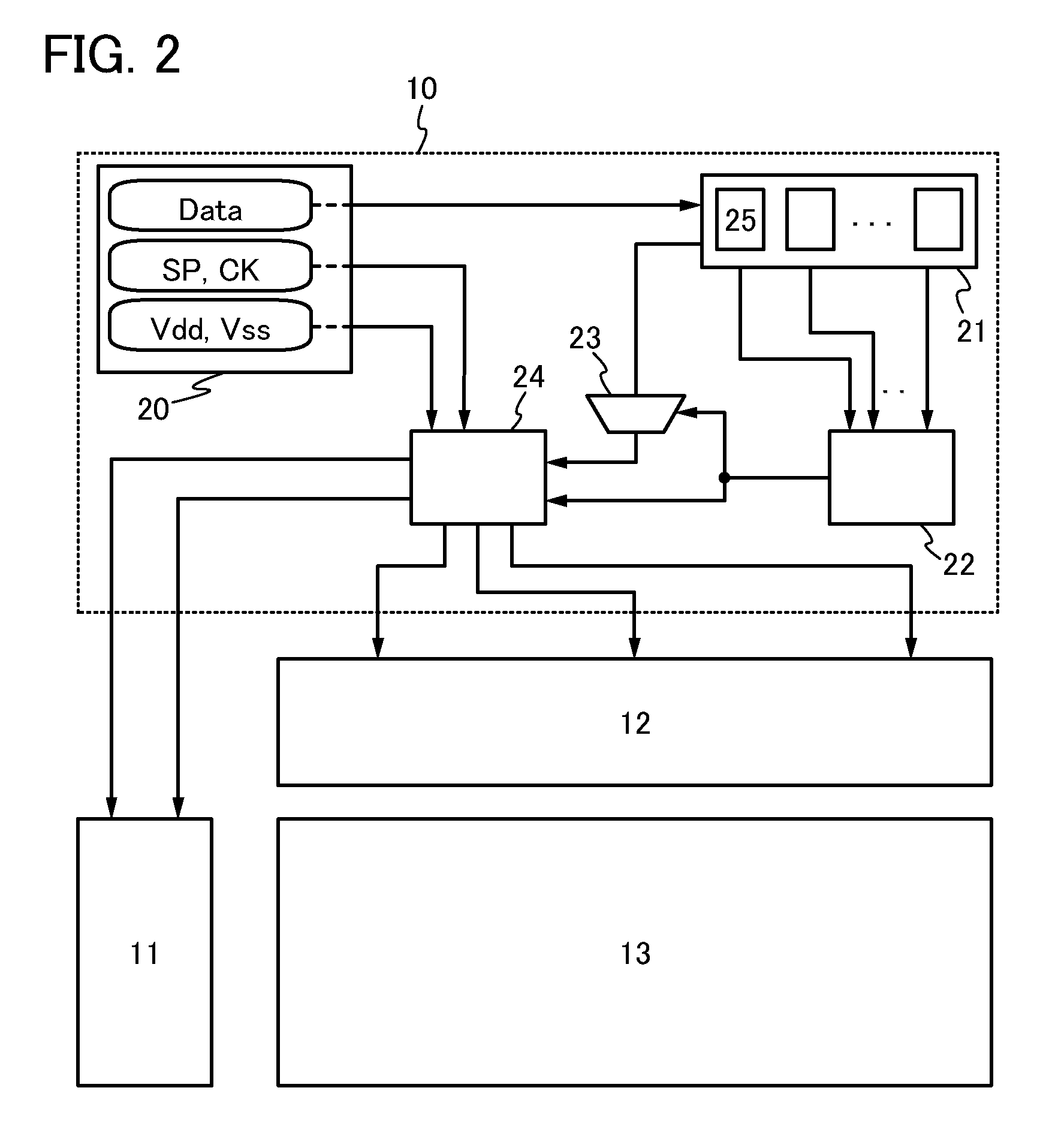
[0028]A structure example of a liquid crystal display device of this embodiment is described below with reference to FIGS. 1A and 1B. FIGS. 1A and 1B illustrate a structure example of a liquid crystal display device. The liquid crystal display device illustrated in FIG. 1A includes a control circuit 10, a scan line driver circuit 11, a signal line driver circuit 12, and a pixel portion 13. The pixel portion 13 includes a plurality of pixels 14 arranged in a matrix form. FIG. 1B illustrates a structure example of one of the pixels 14. The pixel 14 illustrated in FIG. 1B includes a transistor 15 having a gate terminal electrically connected to the scan line driver circuit 11, and a first term...

embodiment 2

[0057]In this embodiment, an example of the transistor in Embodiment 1 is described with reference to FIGS. 4A to 4D.

[0058]FIGS. 4A to 4D illustrate examples of a specific structure and a process for manufacturing the transistor in Embodiment 1. Note that a thin film transistor 410 illustrated in FIGS. 4A to 4D has a bottom-gate structure called a channel-etched type and is also referred to as an inverted-staggered thin film transistor. Although a single-gate thin film transistor is illustrated in FIGS. 4A to 4D, a multi-gate thin film transistor including a plurality of channel formation regions can be formed as needed.

[0059]A process for manufacturing the thin film transistor 410 over a substrate 400 is described below with reference to FIGS. 4A to 4D.

[0060]First, a conductive film is formed over the substrate 400 having an insulating surface, and then, a gate electrode layer 411 is formed through a first photolithography step. Note that a resist mask used in the step may be forme...

embodiment 3

[0114]In this embodiment, a structure of the liquid crystal display device described in Embodiment 1 which has a touch-panel function is described with reference to FIGS. 5A and 5B.

[0115]FIG. 5A is a schematic view of a liquid crystal display device of this embodiment. FIG. 5A illustrates a structure in which a touch panel unit 502 is stacked on a liquid crystal display panel 501 which is the liquid crystal display device of Embodiment 1 and they are attached with a housing 503. As the touch panel unit 502, a resistive touch sensor, a surface capacitive touch sensor, a projected capacitive touch sensor, or the like can be used as appropriate.

[0116]The liquid crystal display panel 501 and the touch panel unit 502 are manufactured separately and stacked as illustrated in FIG. 5A, whereby the cost of manufacturing a liquid crystal display device having a touch-panel function can be reduced.

[0117]FIG. 5B illustrates a structure of a liquid crystal display device having a touch-panel fun...


PUM


Abstract

To reduce power consumption and suppress display degradation of a liquid crystal display device. To suppress display degradation due to an external factor such as temperature. A transistor whose channel formation region is formed using an oxide semiconductor layer is used for a transistor provided in each pixel. Note that with the use of a high-purity oxide semiconductor layer, off-state current of the transistor at a room temperature can be 10 aA/μm or less and off-state current at 85° C. can be 100 aA/μm or less. Consequently, power consumption of a liquid crystal display device can be reduced and display degradation can be suppressed. Further, as described above, off-state current of the transistor at a temperature as high as 85° C. can be 100 aA/μm or less. Thus, display degradation of a liquid crystal display device due to an external factor such as temperature can be suppressed.

Description

TECHNICAL FIELD[0001]The present invention relates to a liquid crystal display device and an electronic device including the liquid crystal display device.BACKGROUND ART[0002]Liquid crystal display devices are widely used for display devices ranging from large-sized display devices such as television sets to small-sized display devices such as mobile phones. Therefore, the development of liquid crystal display devices is intended to achieve cost reduction or to provide high-value added liquid crystal display devices. In recent years in particular, there has been a growing interest in global environment and the development of liquid crystal display devices consuming less power has thus attracted attention.[0003]Technique for reducing power consumption in a liquid crystal display device is disclosed in Patent Document 1. Specifically, a liquid crystal display device is disclosed in which all data signal lines are electrically separated from a data signal driver in an inactive period w...

Claims


Application Information

Patent Timeline
IPC IPC(8): G02F1/1343
CPCG09G3/3648G09G2310/04G09G2320/0214G09G2320/103H01L27/1225H01L29/7869G02F1/1368G02F1/13338H01L27/1214H01L29/786H01L29/66742H01L29/78609G06F3/044H01L21/02483G02F1/136286G06F3/0412G06F3/045G09G3/3677G09G2300/0426G09G2310/08G09G2320/0247G09G2320/043G09G2330/021H01L27/1255
Inventor YAMAZAKI, SHUNPEI
Owner SEMICON ENERGY LAB CO LTD
Why Eureka
Try Eureka