

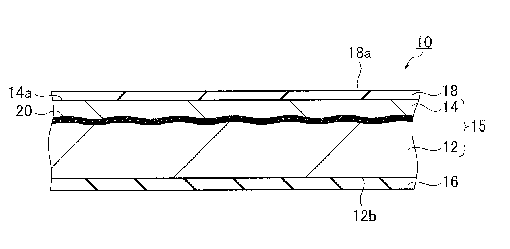
Substrate for selenium compound semiconductors, production method of substrate for selenium compound semiconductors, and thin-film solar cell
a technology of selenium compound semiconductors and substrates, which is applied in the direction of solid-state diffusion coatings, transportation and packaging, coatings, etc., can solve the problems of reducing the quality of formed cigs layers, corroding stainless steel, and reducing so as to prevent corrosion and maintain the strength of the substrate , the effect of not reducing the productivity
- Summary
- Abstract
- Description
- Claims
- Application Information
AI Technical Summary
Benefits of technology
Problems solved by technology
Method used
Image

Examples
example 1
[0225]Example 1 of the substrate for selenium compound semiconductors of the present invention will be specifically described below.
[0226]In this embodiment, the object produced as follows was used as experimental example No. 1. In experimental example No. 1, the substrate body used was constructed of an aluminum base of purity 4N formed on a steel base of SUS430 ferritic stainless steel. The thickness of the steel base was 100 μm, and the thickness of the aluminum base was 30 μm. The substrate body was formed by pressurizing and bonding of the aluminum base to the steel base.
[0227]A protective sheet was pasted onto the rear surface and side surfaces of the steel base so that the steel base did not directly contact the solution. After that, the substrate body was immersed together with an aluminum opposing electrode into a solution of 0.1M oxalic acid adjusted to temperature 16° C., and then DC voltage of 40 V was applied for 1 hour, causing anodization of the aluminum base of the s...
example 2
[0252]In this example 2, the same substrate body as experimental example No. 1 was used, except that the steel base was austenitic stainless steel of thickness 100 μm, which differs from experimental example No. 1 of example 1 above. An oxide film was formed on this substrate body under the same conditions as experimental example No. 1. On the oxide film, a soda lime glass layer, molybdenum film and CIGS layer were laminated in that order under the same conditions as experimental example No. 1, thus producing experimental example No. 11.
[0253]The back surface of the substrate after CIGS layer formation of experimental example No. 11 was objectively visually observed and was observed by microscope (200× magnification). As a result, similar to experimental example No. 1, there was nothing seen attached to the back surface of the substrate in objective visual observation, and there was no evidence that selenium reacted with the back surface of the substrate in observation by microscope...
example 3
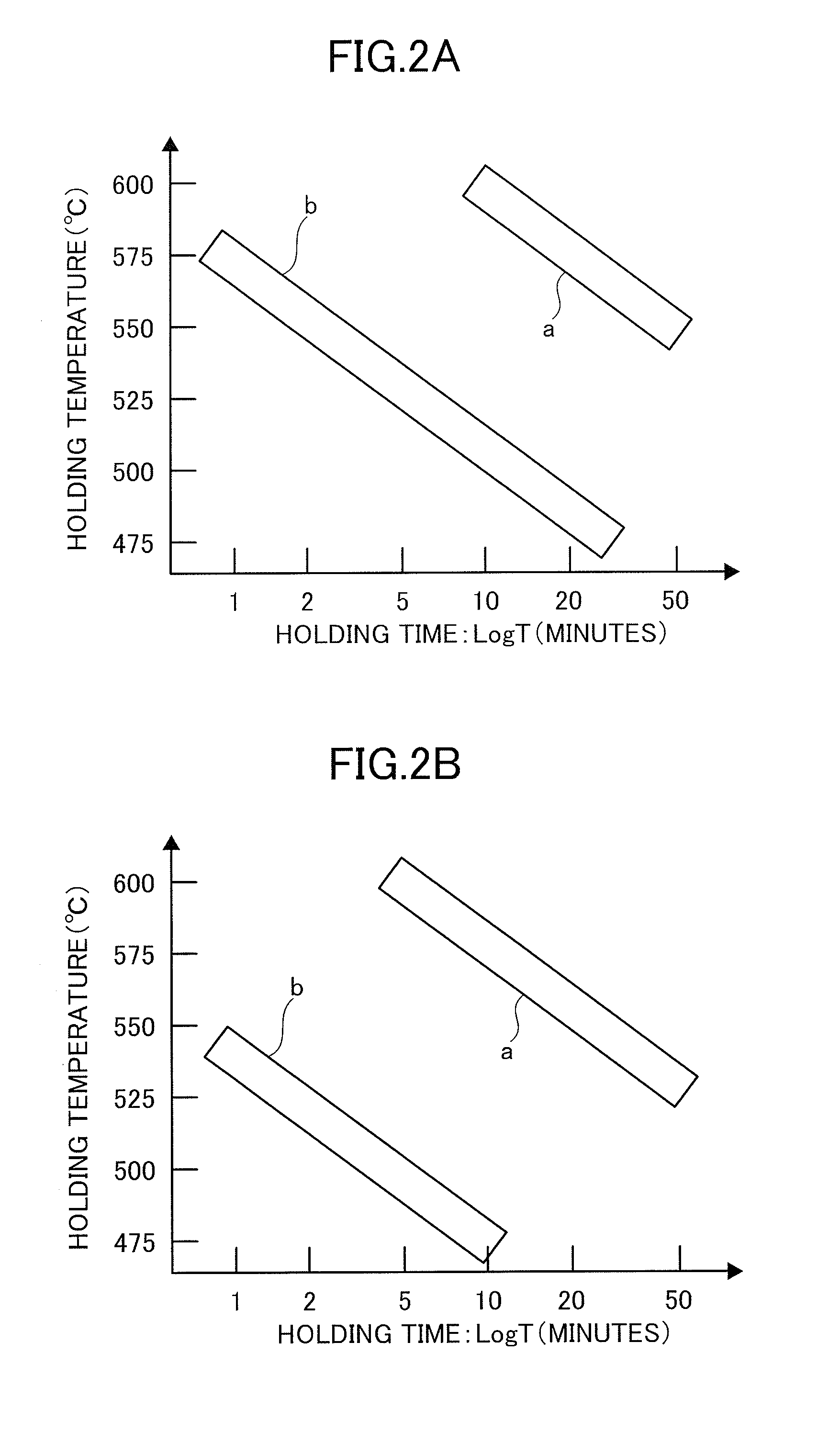
[0258]In this example 3, thermal oxidation treatment was performed on sample A and sample B shown below while varying the heating temperature. The thickness of the oxide film and the thickness of the alloy layer formed at each temperature in sample A and sample B on which thermal oxidation treatment was performed were measured, and cross-sections of the samples were observed. The oxide film thickness results at each temperature are shown in FIG. 9 and FIG. 10.
[0259]Note that the thickness of the oxide film was determined by Auger electron spectroscopy, similar to experimental example No. 1 described above. Also, the thermal oxidation treatment was performed in a theoretical air atmosphere (N2 gas:O2 gas=4:1).
[0260]Observation and alloy layer thickness measurement of samples A and B after thermal oxidation treatment were performed as follows.
[0261]First, samples A and B after thermal oxidation treatment were sectioned by a diamond cutter, after which figuring was performed by ion pol...
PUM
| Property | Measurement | Unit |
|---|---|---|
| thickness | aaaaa | aaaaa |
| thickness | aaaaa | aaaaa |
| thickness | aaaaa | aaaaa |
Abstract
Description
Claims
Application Information