Device, image processing device and method for optical imaging

a technology of optical imaging and image processing, applied in the field of optical imaging devices, image processing devices and methods, can solve the problems of limiting further, reducing the capability of current manufacturing technologies, and reducing so as to reduce the building length of imaging devices, short focal length of each individual channel, and high image resolution capability

Active Publication Date: 2011-09-22
FRAUNHOFER GESELLSCHAFT ZUR FOERDERUNG DER ANGEWANDTEN FORSCHUNG EV
View PDF14 Cites 193 Cited by
  • Summary
  • Abstract
  • Description
  • Claims
  • Application Information

AI Technical Summary

Benefits of technology

[0024]It is thus an advantage of the present invention that the parallel detection of partial areas of the object field in separate optical channels allows a short focal length of each individual channel and thus a reduction of the building length of the imaging device for an expanded object field. Further, the short focal length in connection with a small object field with regard to the overall object field enables, for a respective single channel, the use of simple optical components (for example a refractive lens with a low vertex or angular point) per channel. Further, it is advantageous that the maximum visual field is determined by the lateral dimensions (for example the number of channels) and is thus basically independent of the building or assembly length or of the complexity of the optical setup of each individual channel. Due to the overlap of the detection areas of the optical channels, apart from that a high image resolution capability is achieved compared to the standard artificial compound eyes. Further, an optical device may be generated ac

Problems solved by technology

The existing optics design solutions are characterized by few, but complex (usually aspherical) lens forms which exhaust the possibilities of current manufacturing technologies.
By unsatisfactory measurement methods for quality control of such complex areas and the highly precise lateral and axial mounting accuracies which are needed to take up the optical components of such a miniaturized camera lens or objective are restricted further when implementing the same.
Existing solutions for miniaturized camera modules either do not meet the requirements of specifications or the expectations of integrators and users regarding costs.
This method may, however, not be applied for the manufacturing of miniaturized objectives with a building size of smaller than 5×5×5 mm3 in a sufficient adjustment accuracy.
Further problems result for the supply and the mounting and connecting technology of such small components.
In detail, problems regarding the handling of the components result due to electrostatic forces (small weight and dimensions of the devices) and the danger of contaminating and scratching the sensitive optical surfaces.
For these reasons, more than 80% of production costs are due to assembly processes.
There are advanced approaches regarding the handling of smaller optics in hybrid mounting technology (sensorically supported mechanical and electrostatic as well as pneumatic micro grippers), however the same increase the cost for large-scale manufacturing substantially (e.g. camera optics for mobile telephones).
This leads to a further increase in the unit price.
The main disadvantages of using these manufacturing methods

Method used


Image

  • Device, image processing device and method for optical imaging
  • Device, image processing device and method for optical imaging
  • Device, image processing device and method for optical imaging

Examples


first embodiment

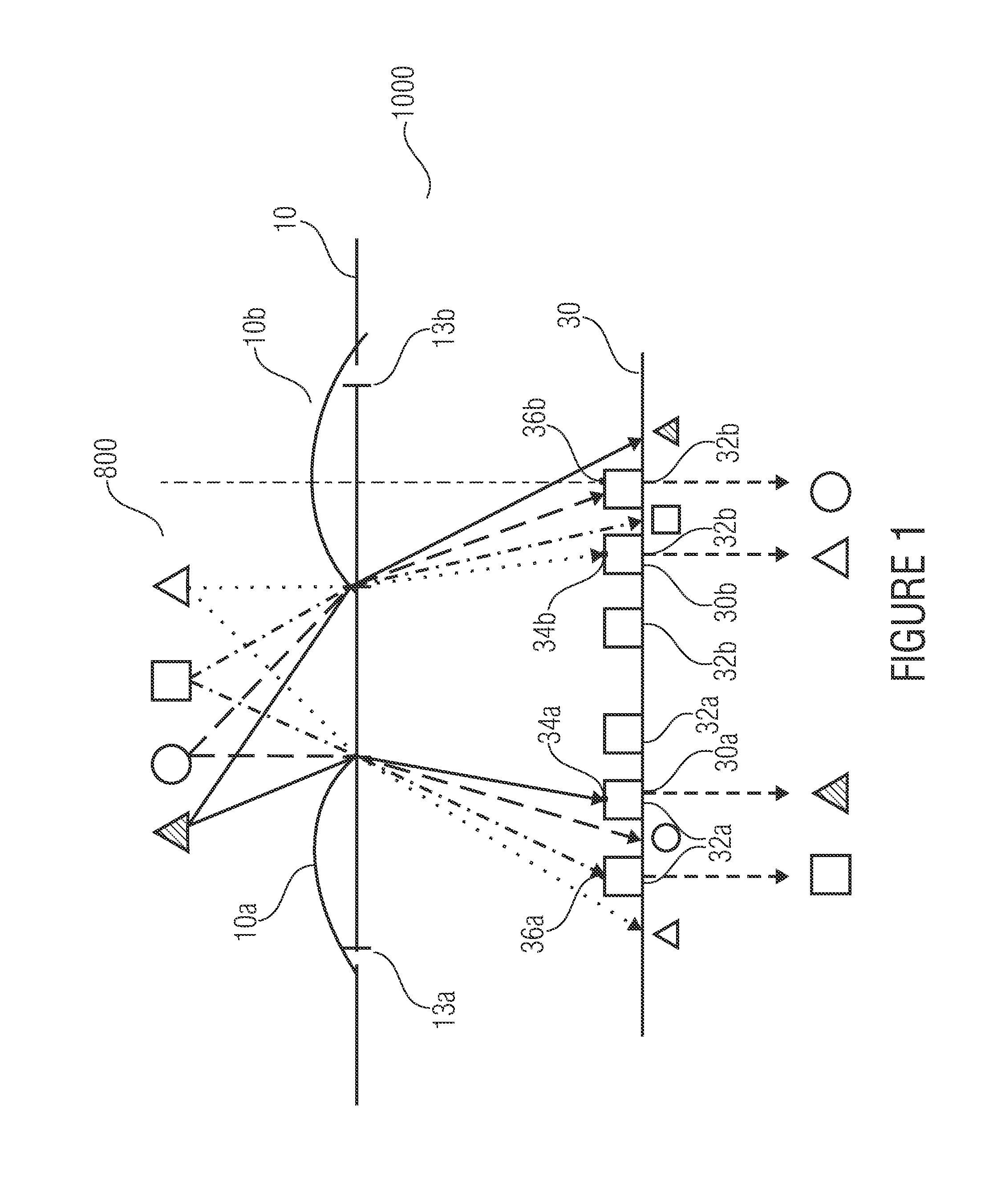
[0046]FIG. 1 shows a schematical illustration of an optical imaging device 1000 according to the present invention. The optical imaging device 1000 includes a micro lens field 10 with a first micro lens 10a and a second micro lens 10b. An image sensor 30 is located below the micro lens field 10. This image sensor 30 includes a first image detector matrix 30a and a second image detector matrix 30b. Each of the two image detector matrices 30a and 30b includes a plurality, for example, of three image detectors 32a, 32b. The first micro lens 10a is associated with the first image detector matrix 30a and forms a first optical channel with the same, the second micro lens 10b is associated with the second image detector matrix 30b and forms a second optical channel with the same. The centers 34a and 34b of the image detector matrices 30a and 30b are offset laterally with respect to the centroids, projected onto the image detector matrices 30a and 30b, of the micro lens apertures 13a and 13...

case 1

[0060]In case 1, the sampling grids of two neighboring channels each are shifted with respect to each other by half of the sampling interval dA of an individual channel (shift: dV). The shift dV of the sampling grid of one of the channels of the considered pair to the respectively next channel of a neighboring pair is a non-integer multiple of the sampling interval in the single channel (for example (N−1 / 2)×dA, wherein N is an integer number). This case is relevant for a small number of optical channels (e.g. 2×2 channels) or also for smaller object distances (smaller than 50× focal length), to guarantee a gapless equidistant sampling of the object field. In other words, a shifting by an odd multiple of half of the sampling interval of a single channel takes place.

case 2

[0061]Case 2 shows a shift dV of the optical channels or the centers of the photo detector matrices of the optical channels by half of the overall sum of all sampling intervals (N×dA) within a channel or by half of the product of the number (N) of the photodiodes and the sampling interval (dA) of an optical channel (for example N×dA / 2), with at the same time an odd number of photodiodes or sampling areas per channel (N). This case is relevant for a larger number of channels to halve the sampling period in the cooperation of neighboring channels and here to obtain neither sampling gaps nor multi-sampling. This characteristic has several advantages. A first advantage is that a shortening (e.g. halving) of the building length (even for the multi-channel system) is enabled with a constant angular sampling. This means that the angular distance, projected retrally by the optics, between two neighboring image pixels of the overall image is maintained. This applies when the same f-stop (F / #...


PUM


Abstract

An optical device for imaging is disclosed having at least one micro lens field with at least two micro lenses and one image sensor with at least two image detector matrices. The at least two image detector matrices each include a plurality of image detectors and there is an allocation between the image detector matrices and the micro lenses, so that each micro lens together with an image detector matrix forms an optical channel. The center points of the image detector matrices are shifted laterally by different distances, with respect to centroids, projected onto the image detector matrices, of the micro lens apertures of the associated optical channels, so that the optical channels have different partially overlapping detection areas and so that an overlapping area of the detection areas of two channels is imaged onto the image detector matrices offset with respect to an image detector raster of the image detector matrices. Further, an image processing device and a method for optical imaging are described.

Description

CROSS-REFERENCE TO RELATED APPLICATIONS[0001]This application claims priority from German Patent Application No. 102009049387.5-31, which was filed on Oct. 14, 2009, and is incorporated herein in its entirety by reference.BACKGROUND OF THE INVENTION[0002]The present invention relates to a device, an image processing device and a method for optical imaging which may, for example, be used in miniaturized camera systems for portable terminal devices.[0003]The use of miniaturized camera systems for portable terminal devices (mobile telephone, PDA, laptop, etc.), apart from the miniaturization of electronic and optoelectronic devices, also requires the miniaturization of the imaging objectives or lenses. Preconditions for this are short lengths of the objective and a small number of optical components (in particular lens elements). The increasing reduction of the image sensor diagonal, which is supported by the development of semiconductor patterning technology (smaller photodiodes equal...

Claims


Application Information

Patent Timeline
IPC IPC(8): H04N5/217H01L27/146
CPCG02B3/0056H04N5/3572H04N5/23229H04N5/2254G02B27/0025H04N23/80
Inventor BRUECKNER, ANDREASDUPARRE, JACQUESWIPPERMANN, FRANKDANNBERG, PETERBRAEUER, ANDREAS
Owner FRAUNHOFER GESELLSCHAFT ZUR FOERDERUNG DER ANGEWANDTEN FORSCHUNG EV
Why Eureka
Try Eureka