Pulse wireless communication device

a wireless communication device and impulse-type technology, applied in multiplex communication, waveguide horns, electromagnetic wave modulation, etc., can solve the problems of high cost of devices that require all of the individual circuits to exhibit ultra-wideband characteristics, incompatible configurations with complicated circuit configurations, and undesirable configurations of microwave/milliwave band devices. achieve the effect of low cost, simple structure and large signal-to-noise ratio

Active Publication Date: 2011-10-20
NAT INST OF INFORMATION & COMM TECH +1
View PDF6 Cites 8 Cited by
  • Summary
  • Abstract
  • Description
  • Claims
  • Application Information

AI Technical Summary

Benefits of technology

[0035]Further, in accordance with the invention of claim 4, the monopulse signal generation circuit is integrated into the radiation type oscillator, whereby the issue of multiple reflection between the radiation type oscillator and the monopulse signal generation circuit can be easily avoided, thus enabling the pulse wireless communication device to be realized with a simple structure at relatively low cost.
[0036]Further, in accordance with the invention of claim 5, amplification gain in the IF band is used to amplify an IF signal from direct current possessed by the three-electrode high-frequency amplifying device of the radiation oscillator during oscillating operation and during mixing operation, whereby an IF signal of large signal-to-noise ratio can be established, thus enabling a high-sensitivity pulse wireless communication device to be realized.
[0037]Further, in accordance with the invention of claim 6, a pulse train pattern is defined in the high-frequency pulse signal of the transmitted RF signal and the radiation oscillator itself is used as a correlator, whereby an IF signal of large signal-to-noise ratio can be established, thus enabling a high-sensitivity pulse wireless communication device to be realized.
[0038]Further, in accordance with the invention of claim 7, when the r

Problems solved by technology

However, the inventions described in the aforesaid Non-patent Document 1 and Non-patent Document 2 are configured with the pulse signal generator, wideband filter, and wideband antenna each connected using a transmission line, so that in addition to the problem of transmission line transmission loss, the configuration is undesirable for a microwave/milliwave band device incompatible with a complicated circuit configuration.
In addition, if the group delay characteristics of the individual circuits are not flat across the wideband, distortion will arise in the pulse waveform.
Such ultra-wideband circuits are therefore more difficult to design than narrow band circuits, so that a device that requires all of the individual circuits to exhibit ultra-wideband characteristics becomes high in cost.
While a taper-structure non-resonant type antenna or a multiple-

Method used


Image

  • Pulse wireless communication device
  • Pulse wireless communication device
  • Pulse wireless communication device

Examples


first embodiment

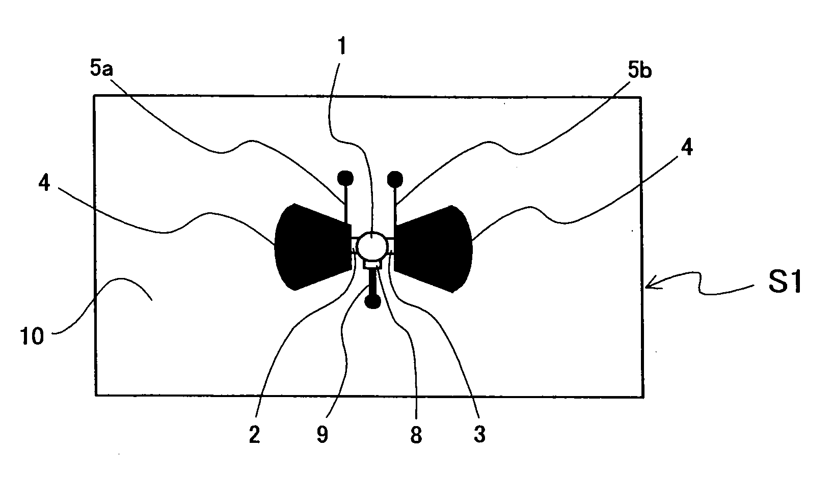
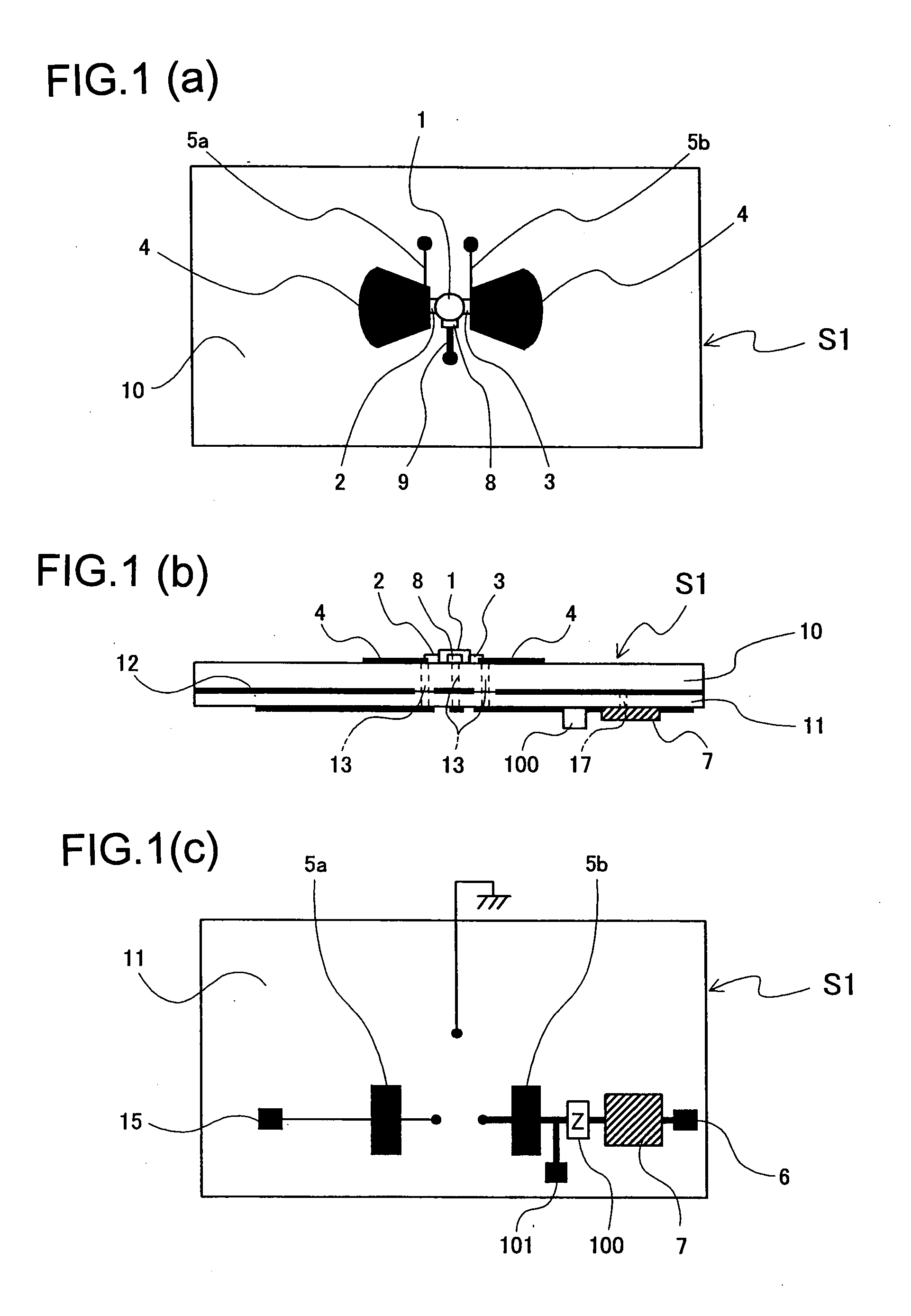
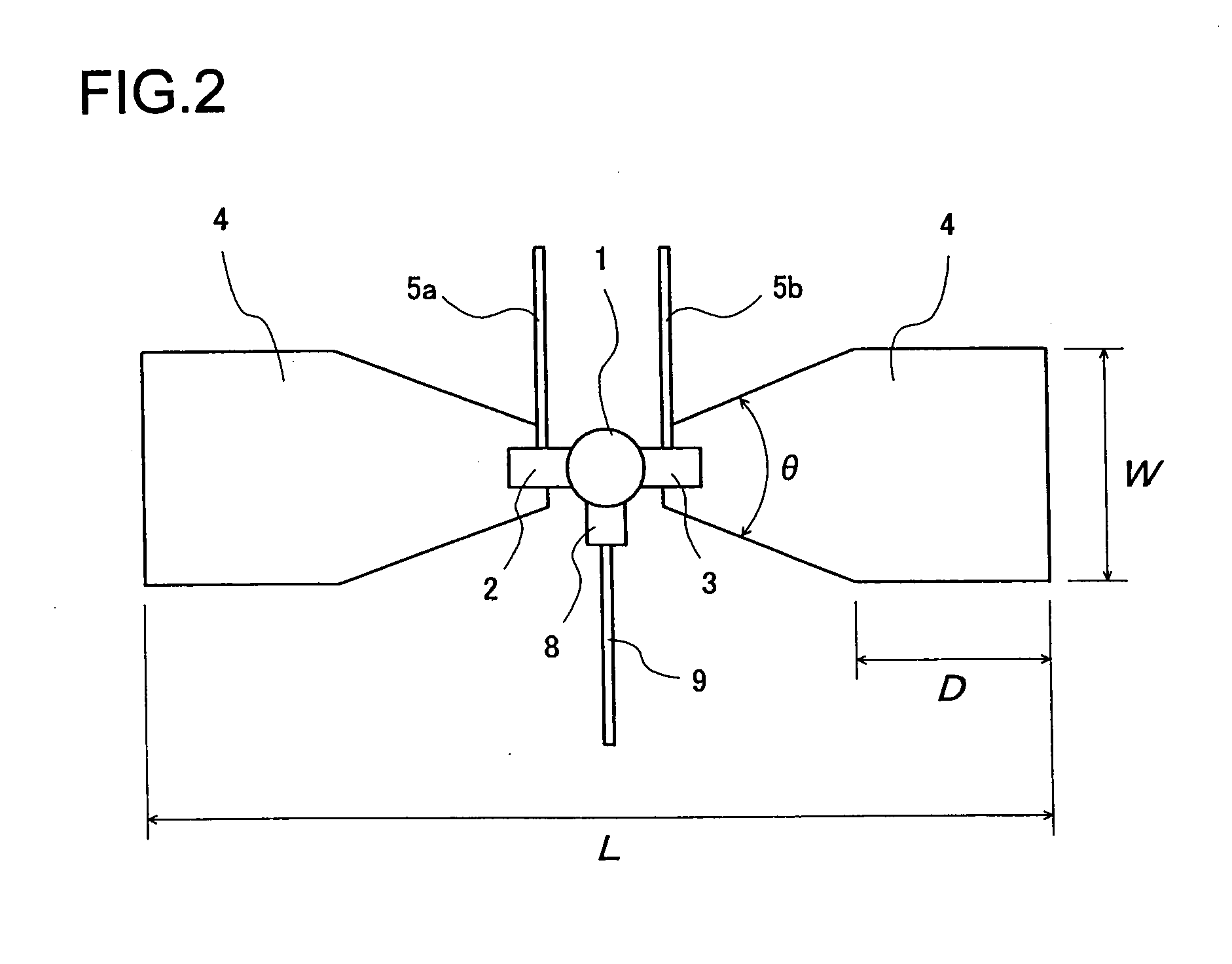
[0065]FIG. 1 shows the basic configuration of a pulse wireless communication device according to a This pulse wireless communication device comprises a radiation type oscillator substrate S1, a signal source that supplies a base band signal thereto (not shown), a power supply that performs DC bias feed (not shown), and a processor that performs analysis and processing of an acquired IF signal (not shown).

[0066]The radiation type oscillator substrate S1 here functions as a “radiation type oscillator that integrates a three-electrode high-frequency amplifying device to generate negative resistance in a resonant cavity and shares an antenna function for radiating an electromagnetic wave into space.” And the high-frequency pulse signal radiated into space by this radiation type oscillator becomes a transmitted RF signal at time intervals and timing based on the transmit data signal. On the other hand, when a received RF signal arriving from an external wireless communication device ent...

second embodiment

[0087]A pulse wireless communication device will be explained next based on FIG. 6.

[0088]The pulse wireless communication device of the present embodiment comprises a radiation type oscillator substrate S2, a signal source that supplies a base band signal thereto (not shown), a power supply that performs DC bias feed (not shown), and a processor that performs analysis and processing of an acquired IF signal (not shown). Further, the radiation oscillator substrate S2 of the pulse wireless communication device of the present embodiment configures the required circuits using a three-layer substrate with an inner-layer GND 12 constituting a grounding conductor layer sandwiched between a front-side dielectric substrate 10 and a rear-side dielectric substrate 11; an RF circuit section of the radiation type oscillator is constituted by the front surface and the inner-layer GND 12; and an RF choke circuit and a base band circuit are constituted by the inner-layer GND 12 and the rear surfac...

third embodiment

[0118]Next, the pulse wireless communication device will be explained based on FIG. 20. The pulse wireless communication device of the present embodiment is provided on a radiation oscillator substrate S3 (whose high-frequency pulse generating and radiating structure is the same as the radiation oscillator substrate S1, S1a, S1b, S1c, S2 or S2a set out in the foregoing and whose operation is also the same) with a Frequency Selective Surface (FSS) as a frequency selective filter means. Further, a grounding conductor structure is provided for preventing leakage of unnecessary signal components of a frequency lower than the frequency of the radiated high-frequency pulse signal (e.g., a base band signal component or monopulse signal component).

[0119]On the radiation direction side of the radiation oscillator substrate S3 is arranged an FSS substrate 31 patterned on the side of the inner surface (surface facing the radiation surface of the radiation oscillator substrate S3) with a low-p...


PUM


Abstract

To provide a microwave/milliwave UWB pulse wireless communication device that enables realization of structural simplification, high performance, compact integration, easy design, low power consumption, and low cost. A radiation type oscillator is configured by a radiation type oscillator substrate S1 equipped with a microwave transistor 1 for generating negative resistance by short-duration operation and a resonant cavity structure, a high-frequency pulse signal of an oscillation frequency/frequency bandwidth determined based on negative resistance produced by the short-duration operation of the microwave transistor 1 and the resonant cavity structure is generated as a transmitted RF signal and simultaneously radiated into space, and the radiation type oscillator is caused to perform oscillating operation when a received RF signal arriving from an external wireless communication device enters the radiation type oscillator, whereby a received data signal is established based on acquisition of an IF signal owing to mixing by the radiation type oscillator itself.

Description

TECHNICAL FIELD[0001]This invention relates to an ultra-wideband (UWB) impulse-type wireless data transmitter-receiver, particularly to a technology for realizing structure simplification, low cost, and high performance in a microwave / milliwave band device incompatible with a complicated circuit configuration.BACKGROUND ART[0002]UWB technologies have attracted attention as communication technologies in recent years. Although these technologies use extremely broad frequency bands, they are extremely low in power spectral density and therefore have the advantage of being able to share frequencies already in use. Moreover, they have advantages such as that by using short pulses of several hundred picoseconds or shorter, they make it possible to perform high-speed data transmission.[0003]In conventional microwave / milliwave band UWB technology, a pulse wireless communication device is configured with a pulse signal generator, wideband filter and wideband antenna each connected using a tr...

Claims


Application Information

Patent Timeline
IPC IPC(8): H04L27/00H01Q1/38H01Q9/28H01Q13/02H01Q13/06H01Q23/00H03C7/02H03D9/06H04B1/04H04B1/38H04B1/3822H04B1/717H04J13/00
CPCH01Q9/265H01Q9/285H01Q13/10Y02B60/50H01Q23/00H03B5/1847H04B1/7174H01Q13/16
Inventor UTAGAWA, HITOSHIMATSUI
Owner NAT INST OF INFORMATION & COMM TECH
Why Eureka
Try Eureka