Electron injection nanostructured semiconductor material anode electroluminescence method and device

an anode electroluminescence and nano-structured technology, applied in the field of electricity to light energy conversion, can solve the problems of narrow spectral lines, limited practice, and multiple led approaches, and achieve low efficiency of green leds

Active Publication Date: 2011-12-08
RGT UNIV OF CALIFORNIA
View PDF20 Cites 46 Cited by
  • Summary
  • Abstract
  • Description
  • Claims
  • Application Information

AI Technical Summary

Benefits of technology

[0010]Embodiments of the invention also include the usage of nanostructured semiconductor materials as phosphors for conventional planar LED and nanowire array light emitting diodes and CFL. For the use in

Problems solved by technology

The multiple LED approach leads to narrow spectral lines and limited in practice by the low efficiency of green LEDs.
On the other hand, conventional blue LEDs coated with yellow phosphors give a cold white light, and are not color tunable.
Another problem with solid state lighting based upon traditional light emitting diode structures is that the traditional solid state LEDs don't fit the power model that has been implemented for in

Method used


Image

  • Electron injection nanostructured semiconductor material anode electroluminescence method and device
  • Electron injection nanostructured semiconductor material anode electroluminescence method and device
  • Electron injection nanostructured semiconductor material anode electroluminescence method and device

Examples


Embodiment Construction

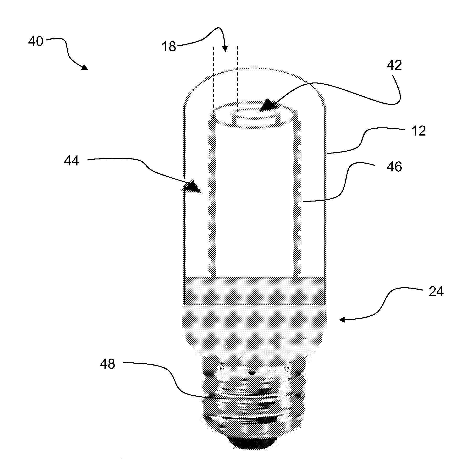
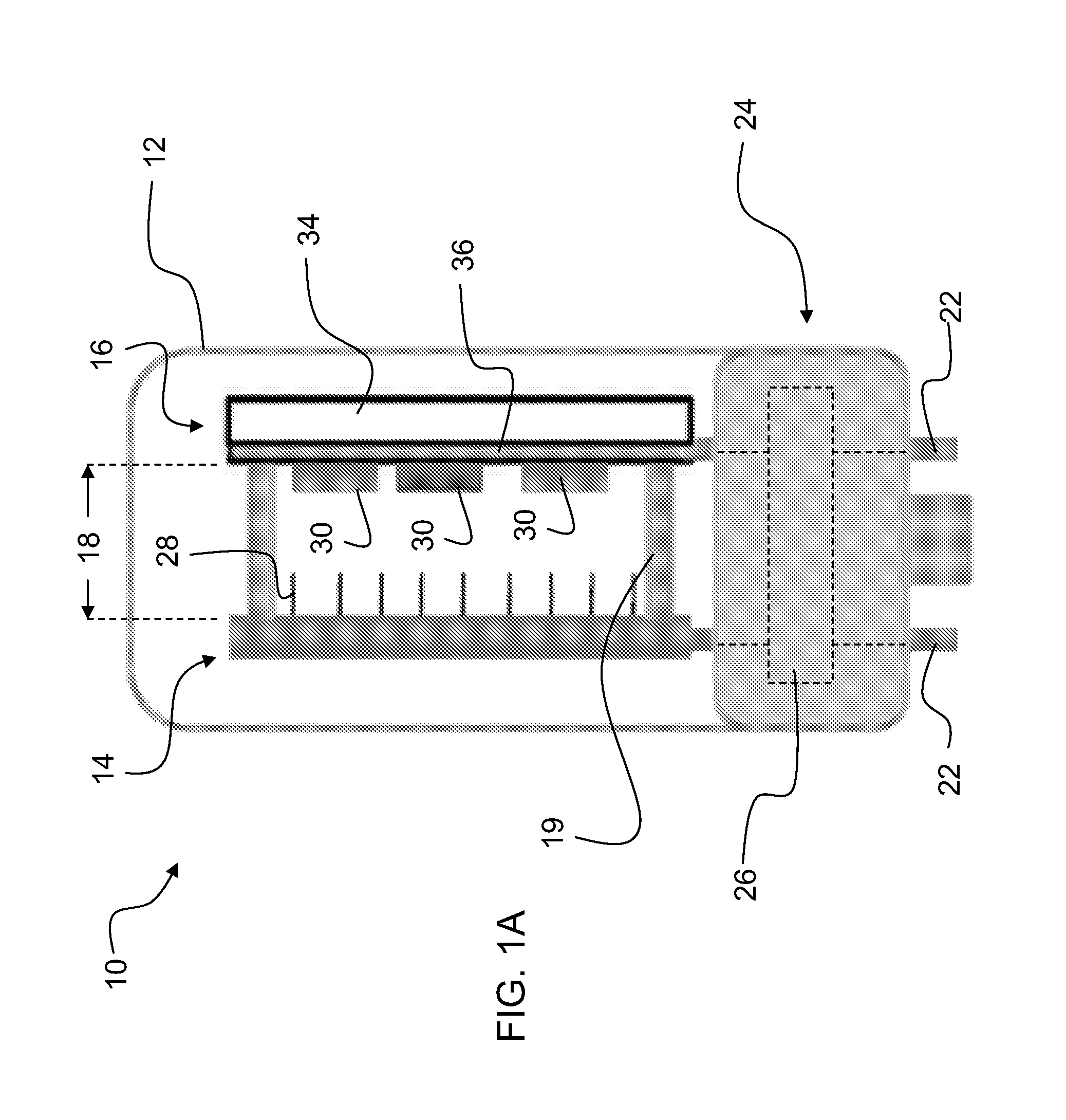
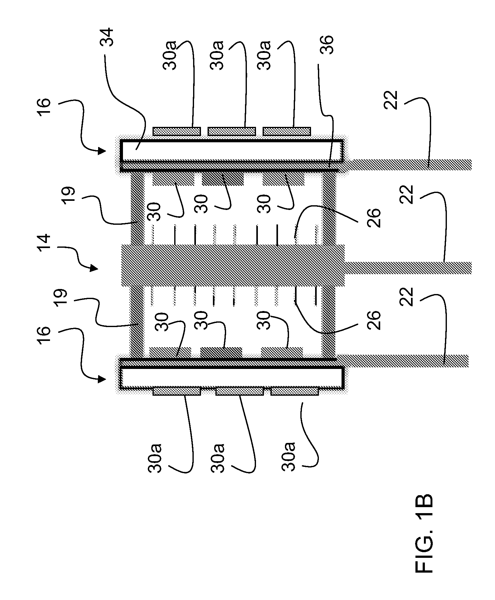
[0015]Embodiments of the invention include methods and devices for producing light by injecting electrons from field emission cathode across a gap into nanostructured semiconductor materials. In methods and devices of the invention, light is not generated by the passing of electrons through a p / n junction, as occurs in conventional light-emitting diodes (LEDs). Instead, the electrons issue from a separate field emitter cathode and are accelerated by a voltage across a gap towards the surface of the nanostructured material that forms part of the anode. At the nanostructure material, the electrons undergo electron-hole (e-h) recombination resulting in a highly efficient electroluminescent (EL) emission.

[0016]In a preferred embodiment lighting device, a vacuum enclosure houses a field emitter cathode. The vacuum enclosure also houses an anode that is separated by a gap from said cathode and disposed to receive electrons emitted from the cathode. The anode includes semiconductor light e...


PUM


Abstract

Embodiments of the invention include methods and devices for producing light by injecting electrons from field emission cathode across a gap into nanostructured semiconductor materials, electrons issue from a separate field emitter cathode and are accelerated by a voltage across a gap towards the surface of the nanostructured material that forms part of the anode. At the nanostructure material, the electrons undergo electron-hole (e-h) recombination resulting in electroluminescent (EL) emission. In a preferred embodiment lighting device, a vacuum enclosure houses a field emitter cathode. The vacuum enclosure also houses an anode that is separated by a gap from said cathode and disposed to receive electrons emitted from the cathode. The anode includes semiconductor light emitting nano structures that accept injection of electrons from the cathode and generate photons in response to the injection of electrons. External electrode contacts permit application of a voltage differential across the anode and cathode to stimulate electron emissions from the cathode and resultant photon emissions from the semiconductor light emitting nanostructures of the anode. Embodiments of the invention also include the usage of nanostructured semiconductor materials as phosphors for conventional planar LED and nanowire array light emitting diodes and CFL. For the use in conventional planar LEDs, the nanostructures may take the form of quantum dots, nanotubes, branched tree-like nanostructure, nanoflower, tetrapods, tripods, axial heterostructures nanowires hetero structures.

Description

PRIORITY CLAIM AND REFERENCE TO RELATED APPLICATION[0001]The application claims priority under 35 U.S.C. §119 from prior U.S. provisional application Ser. No. 61 / 119,938, which was filed on Dec. 4, 2008 and from prior U.S. provisional application Ser. No. 61 / 121,333, which was filed on Dec. 10, 2008.FIELD[0002]A field of the invention is electricity to light energy conversion. Applications of the invention include lighting and displays.BACKGROUND[0003]Meeting the challenge of increasing worldwide demand for energy requires strategies for more efficient energy use as well as sustainable approaches to energy generation and conservation. Lighting is a major contributor to electricity consumption, accounting for 19% of global use and 34% for the U.S. The U.S. lighting market is currently divided among various lamp types as follows: 63% incandescent, 35% fluorescent, 2% halogen. The incandescent light bulb is only 5% efficient (15 lm / W) while the fluorescent lamp has 15-25% efficiency (5...

Claims


Application Information

Patent Timeline
IPC IPC(8): G21H3/02H01L33/04B82Y40/00
CPCH01L33/502H01J63/06H05B33/02H05B33/14
Inventor WANG, DELI
Owner RGT UNIV OF CALIFORNIA
Why Eureka
Try Eureka