

Field Effect Transistor
a field effect transistor and transistor technology, applied in the field of field effect transistors, can solve the problems of insufficient heat resistance of materials, high cost, and high equipment investment, and achieve the effects of excellent characteristics, enhanced carrier mobility, and excellent heat resistan
- Summary
- Abstract
- Description
- Claims
- Application Information
AI Technical Summary
Benefits of technology
Problems solved by technology
Method used
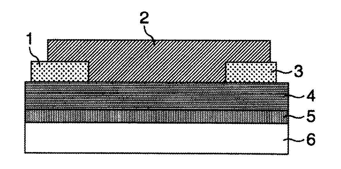
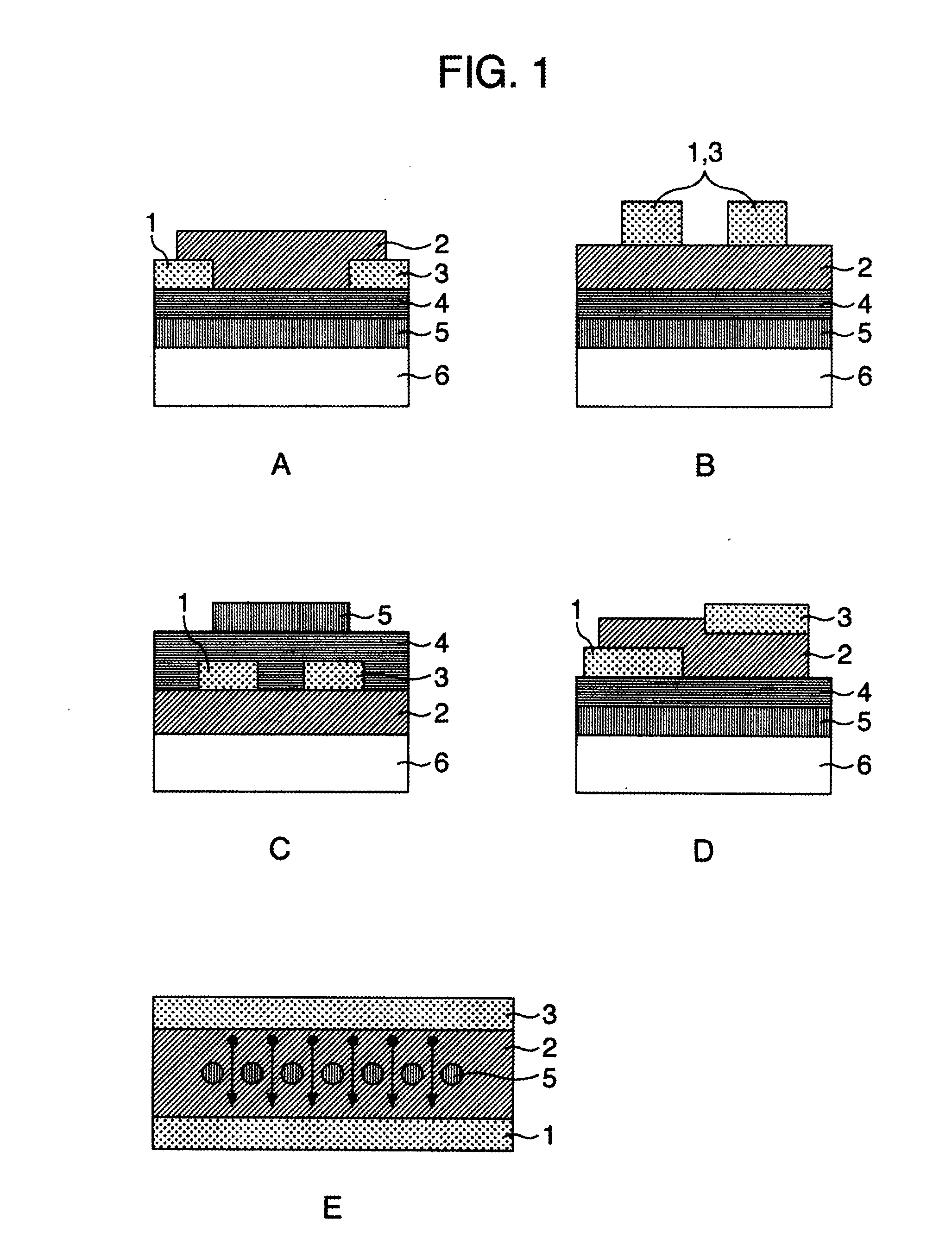
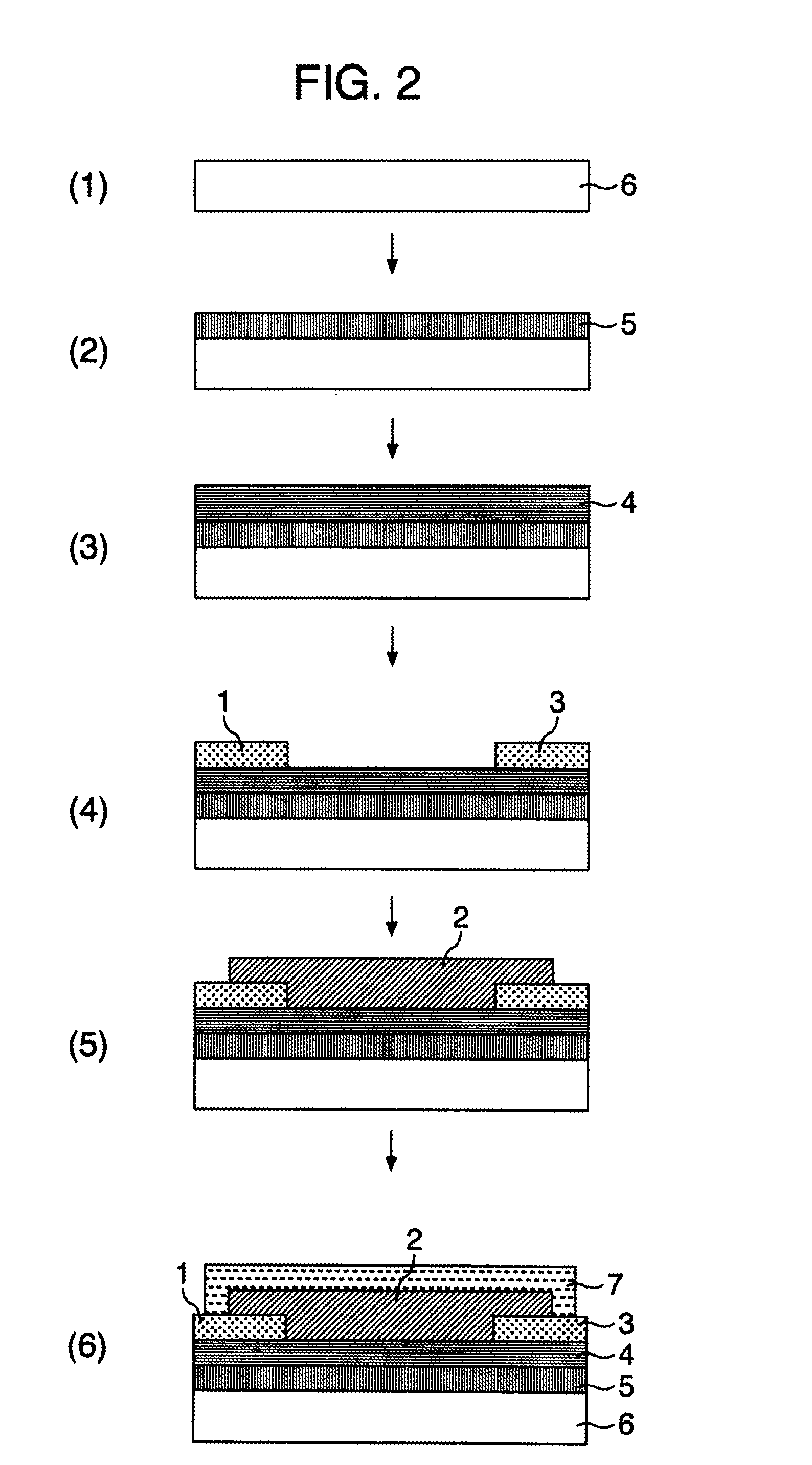
Image

Examples
synthesis example 1
[0135]Synthesis of methyl 6-octynyl-2-naphthoate (100)
[0136]A 50 ml 3-neck flask having a reflux tube and a dripping funnel was substituted with nitrogen, and DMF (8 ml) was added thereinto and bubbled for 10 min. Into the 3-neck flask, methyl 6-bromo-2-naphthoate (1 g, 3.8 mmol), Pd(pph3)4 (218 mg, 0.12 mmol), NEt3 (1.58 ml, 11.3 mmol), and CuI (36 mg, 0.19 mmol) were fed and stirred. Into the dripping funnel, toluene (8 ml) and 1-octyne (0.56 ml, 3.8 mmol) were fed, bubbled with Ar gas for 10 min, and then slowly dripped. Because raw materials still remained after stirring for 27.5 hours at room temperature, 1-octyne (0.28 ml, 1.9 mmol) was further added. After 4 hours, water and 2 N HCl were added so that the reaction was halted at ph 7. After extraction with methylene chloride, the organic phase was dried with anhydrous magnesium and filtered, and then the solvent was distilled away with a rotary evaporator. The reacted mixture produced was isolated and refined with silica gel c...
synthesis example 2
[0139]Synthesis of methyl 6-octyl-2-naphthoate (101)
[0140]Into a 50 ml 3-neck flask, methyl 6-octynyl-2-naphthoate (100) (118 mg, 0.4 mmol) was fed and substitution with Ar gas performed. Then, 10% Pd / C (107 mg, 0.52 mmol) and toluene (25 ml) were added and dissolved. Using an aspirator, H2 gas substitution was performed three times with stirring at room temperature for 2 hours. After completion of the reaction, filtration with celite was performed using hexane and the solvent was distilled away to produce a white solid of 6-octyl-naphthalene methyl carboxylate (107 mg, 0.36 mmol, 90%).
[0141]Methyl 6-octyl-2-naphthoate: white; 1H NMR (270 MHz, CDCl3) δ0.87 (t, 3H, J=6.90 Hz), δ1.27˜1.71 (m, 8H), δ2.79 (t, 2H, J=7.75 Hz) δ3.98(s,3H, CO2CH3) δ7.40 (dd, 1H, J=7.99, 1.66 Hz, ArH) δ7.65 (s, 1H, ArH) δ7.81(d, 1H, J=8.2, ArH) δ7.87 (d, 1H, J=8.84 Hz, ArH) δ8.03 (dd, 1H, J=8.60, 1.75 Hz) ELMS, m / z=298(M+)
synthesis example 3
Synthesis of 2-hydroxymethyl-6-octylnaphthalene (102)
[0142]
[0143]Into a 50 ml 3-neck flask, anhydrous THF (20 ml) and LAH (38 mg, 1 mmol) were added. While the flask was cooled in iced water, anhydrous THF (5 ml) solution of 6-octyl-naphthalene methyl carboxylate (101) (298 mg, 1 mmol) was slowly dripped. After stirring at room temperature for one hour, the reactant was fed into a beaker containing ice (30 ml to 40 ml) and 2 N HCL was added thereto. After complete separation of an organic phase and a water phase, extrusion and subsequent extraction with methylene chloride, the organic phase was dried with anhydrous magnesium. After filtration, the solvent was distilled away with a rotary evaporator to produce white 2-hydroxymethyl-6-octylnaphthalene (270 mg, 1 mmol, 100%).
[0144]2-Hydroxymethyl-6-octylnaphthalene: white; 1H NMR (270 MHz, CDCl3) δ0.87 (t, 3H, J=6.53 Hz), δ1.26˜1.72 (m, 8H), δ2.76 (t, 2H, J=7.71 Hz) δ4.85 (s, 2H, CH2OH) δ7.35 (dd, 1H, J=8.53, 1.20 Hz, ArH) δ7.46 (dd, 1...
PUM
| Property | Measurement | Unit |
|---|---|---|
| particle diameter | aaaaa | aaaaa |
| particle diameter | aaaaa | aaaaa |
| boiling point | aaaaa | aaaaa |
Abstract
Description
Claims
Application Information