Photomask blank, photomask, and method of manufacturing photomask blank

a technology of photomask and blank, which is applied in the field of photomask blank, photomask and photomask manufacturing method, can solve the problems of no optimization, pattern collapsing, etc., and the thickness of the photomask is reduced, and the over-etching time is reduced, and the thickness of the light-shielding film is reduced. , the effect of reducing the thickness of the light-shielding film

Active Publication Date: 2011-12-15
HOYA CORP
View PDF3 Cites 19 Cited by
  • Summary
  • Abstract
  • Description
  • Claims
  • Application Information

AI Technical Summary

Benefits of technology

[0038]It is possible to reduce the thickness of a light-shielding film of a photomask blank in a preferred embodiment of the present invention, and this enables reduction in clear etching time (CET), and in addition, over etching time (OET) is also reduced. In particular, in a photomask blank in a preferred embodiment of the present invention, it is possible to reduce the thickness of a light-shielding film having a structure consisting of a plurality of layers (particularly a three-layer structure) by providing a light-shielding layer (absorption layer) having a high content of a metal such as Cr, and this enables reduction in clear etching time (CET) and over etching time (OET).
[0039]Moreover, in a photomask blank in a preferred embodiment of the present invention, over etching time (OET) can be reduced by combining a film containing a metal (e.g., Cr) having a high etching rate (ER) (antireflection layer) with a metal-containing film having a low etching rate (ER) (absorption layer), by providing a predetermined balance between the thickness of the layer having the high etching rate (ER) and the thickness of the layer having the low etching rate (ER), and by disposing the layer having the low etching rate (ER) at a predetermined position.
[0040]In a photomask blank in a preferred embodiment of the present invention, the thickness of a resist formed on a light-shielding film can be reduced by reducing clear etching time (CET), over etching time (OET) or both of them. As a result, in the photomask blank in the preferred embodiment of the present invention, the problem of pattern collapsing, etc. is not easily caused, and therefore, a fine mask pattern can be formed thereby.
[0041]Moreover, in a preferred embodiment of the present invention, by providing a structure in which a plurality of layers having a different metal content with a predetermined thickness are laminated, it is possible to provide a photomask blank comprising a light-shielding film having a predetermined thickness by which a sufficient optical density can be provided, wherein the etching rate (ER) of the entire light-shielding film is high.

Problems solved by technology

However, when the resist film thickness is increased, the aspect ratio is increased, and this causes the problem of pattern collapsing, etc., particularly in the case where a fine pattern is to be formed.
However, regarding the above-described CrON film, it is just that the optical density per unit film thickness at a wavelength of 450 nm is set, and regarding a wavelength of exposure light equal to or less than wavelength of an ArF excimer laser light, no optimization has been made.
In particular, in the case of hyper-NA lithography, the angle of light incidence relative to a photomask becomes shallower, and this causes the problem that a miniaturized mask pattern itself shades a transfer image (shadowing).
In addition, the cross-section shape is prone to vary, and this, together with shadowing, causes reduction of transfer accuracy of CD (Critical Dimension).[Patent Document 1] Japanese Laid-Open Patent Publication No. 2007-33470

Method used


Image

  • Photomask blank, photomask, and method of manufacturing photomask blank
  • Photomask blank, photomask, and method of manufacturing photomask blank
  • Photomask blank, photomask, and method of manufacturing photomask blank

Examples


first embodiment

1. First Embodiment

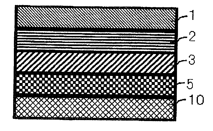
[0050]The photomask blank according to the first embodiment of the present invention is a photomask blank for producing a photomask to which an ArF excimer laser light is applied, wherein:

[0051]a thin film having a multilayer structure is provided on a light transmissive substrate; and

[0052]the uppermost layer of the thin film has an amorphous structure made of a material comprising chromium and at least one of nitrogen, oxygen and carbon.

1.1. Light Transmissive Substrate

[0053]The light transmissive substrate is not particularly limited as long as it is a substrate that is light-transmissive. Examples thereof include a quartz glass substrate, an aluminosilicate glass substrate, a calcium fluoride substrate, and a magnesium fluoride substrate. Among them, the quartz glass substrate is preferred, because it has a high flatness level and a high smoothness level, and because, when transferring a pattern to a semiconductor substrate using a photomask, distortion of a t...

second embodiment

2. Second Embodiment

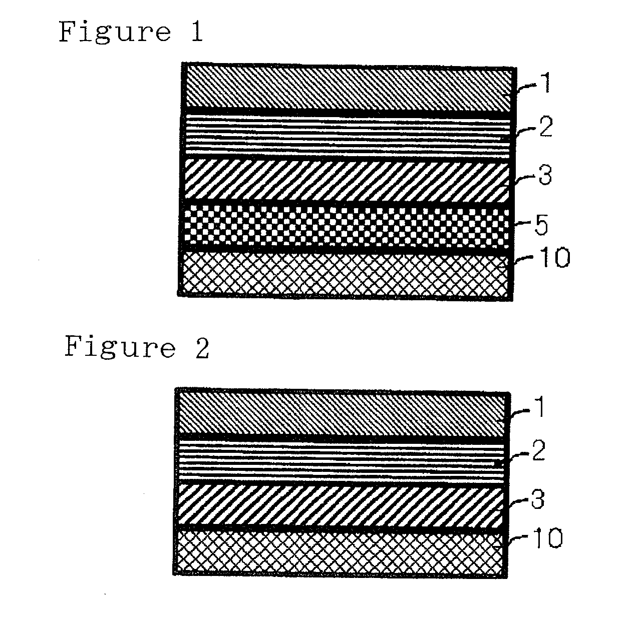
[0110]At the time of processing a light-shielding film formed on a light transmissive substrate, the present inventors found the following matters:[0111](1) in the case of a two-layer structure consisting of a light-shielding layer and a front-surface antireflection layer, when the light-shielding layer that is a lower layer is formed with a material having a low etching rate, longer over etching time is required, and as a result, the total etching time is increased, whereas when the lower layer is formed with a material having a high etching rate, clear etching time is reduced, but there is a case where over etching time is increased due to loading, and thus, it is difficult to reduce etching time when using the two-layer structure;[0112](2) in order to reduce over etching time, it is preferred to employ a three-layer structure consisting of a back-surface antireflection layer, a light-shielding layer and a front-surface antireflection layer, wherein a material ...

third embodiment

3. Third Embodiment

[0130]When oxygen is included in a metal-containing layer which constitutes a light-shielding film, the etching rate is increased, but the optical density per unit film thickness is decreased, and as a result, the thickness of the light-shielding layer is increased. Further, in the case of a film having a single speed in which there is no difference of etching rate in the longitudinal direction, variation of the cross-section shape due to loading tends to easily occur.

[0131]Further, in the case of a photomask exposed to an ArF excimer laser light, it preferably has a structure having a back-surface antireflection layer and a front-surface antireflection layer in order to prevent reduction of the pattern accuracy caused because reflected light from a transferred product such as a semiconductor substrate returns to the transferred product. However, in the case where a light-shielding film having such a laminated structure is designed with the limitation in which the...


PUM

PropertyMeasurementUnit
thicknessaaaaaaaaaa
thicknessaaaaaaaaaa
thicknessaaaaaaaaaa

Abstract

The present invention provides a photomask blank for producing a photomask to which an ArF excimer laser light is applied, wherein: a thin film having a multilayer structure is provided on a light transmissive substrate; and the uppermost layer of the thin film has an amorphous structure made of a material comprising chromium and at least one of nitrogen, oxygen and carbon.

Description

TECHNICAL FIELD[0001]The present invention relates to a photomask blank, a photomask and a method for manufacturing a photomask blank.BACKGROUND ART[0002]In general, in the production processes of high-density semiconductor integrated circuits such as LSI, color filters for CCD (charge-coupled device) and LCD (liquid crystal display device), magnetic heads, etc., microfabrication utilizing the photolithographic technique using photomasks is performed.[0003]In this microfabrication, a photomask, in which a light-shielding film made of a metal thin film such as a chromium film is generally formed on a light transmissive substrate made of quartz glass, aluminosilicate glass or the like by means of sputtering, vacuum deposition or the like to provide a photomask blank, wherein the light-shielding film is formed to have a predetermined pattern, is used.[0004]A photomask is produced using such a photomask blank with the following processes: an exposure process in which a desired pattern e...

Claims


Application Information

Patent Timeline
Patent Type & Authority Applications(United States)
IPC IPC(8): G03F1/00
CPCG03F1/46G03F1/22G03F1/54H01L21/0274G03F1/80G03F1/50H01L21/0273H01L21/0276
Inventor IWASHITA, HIROYUKISHISHIDO, HIROAKIKOMINATO, ATSUSHIHASHIMOTO, MASAHIROHOSOYA, MORIO
Owner HOYA CORP
Why Eureka
Try Eureka