Microbolometer for infrared detector or Terahertz detector and method for manufacturing the same

Inactive Publication Date: 2011-12-29
UNIV OF ELECTRONIC SCI & TECH OF CHINA
View PDF2 Cites 46 Cited by
  • Summary
  • Abstract
  • Description
  • Claims
  • Application Information

AI Technical Summary

Benefits of technology

[0011]The problem to be resolved in the present invention is to provide a microbolometer and method for manufacturing the same, which is capable of overcoming the shor

Problems solved by technology

However, the electric structure of the vanadium atom is 3d34s2, wherein 4s and 3d orbits can lose some or all electrons, so the vanadium oxide films prepared by the conventional method have some inherent shortcomings of complex valence of element V in the vanadium oxide films, and poor stability of the chemical structures of the films.
Since element V has the complex composition, slight fluctuation in the preparation process might greatly impact on the chemical compositions of the vanadium oxide films, so that the electrical, optical and mechanical properties of the films are significantly changed, thereby affecting the performance of the device.
Therefore, the main shortcomings of the microbolometer based on the vanadium oxide films are that the preparation is difficult, and the repeatability and stability of the product are poor.
However, the carbon nanotubes, especially the carbon nanotubes reclining on the surface of the substrate have non-ideal infrared absorbing performance (referring to Z. Wu, Z. Chen, et al., “Transparent, Conductive Carbon Nanotube Films”, Science, 305, 1273-1276 (2004)).
This shortcoming will seriously impact on the performance of related device.
However, this structure based on the single carbon nanotubes has an obvious s

Method used


Image

  • Microbolometer for infrared detector or Terahertz detector and method for manufacturing the same
  • Microbolometer for infrared detector or Terahertz detector and method for manufacturing the same
  • Microbolometer for infrared detector or Terahertz detector and method for manufacturing the same

Examples


Embodiment Construction

[0101]The present invention is further explained in detail with the accompanying drawings.

[0102]I The Method for Manufacturing the Composite Material of the One-Dimensional Carbon Nanotubes and Two-Dimensional Vanadium Oxide Film

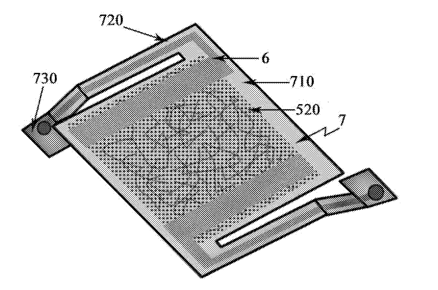
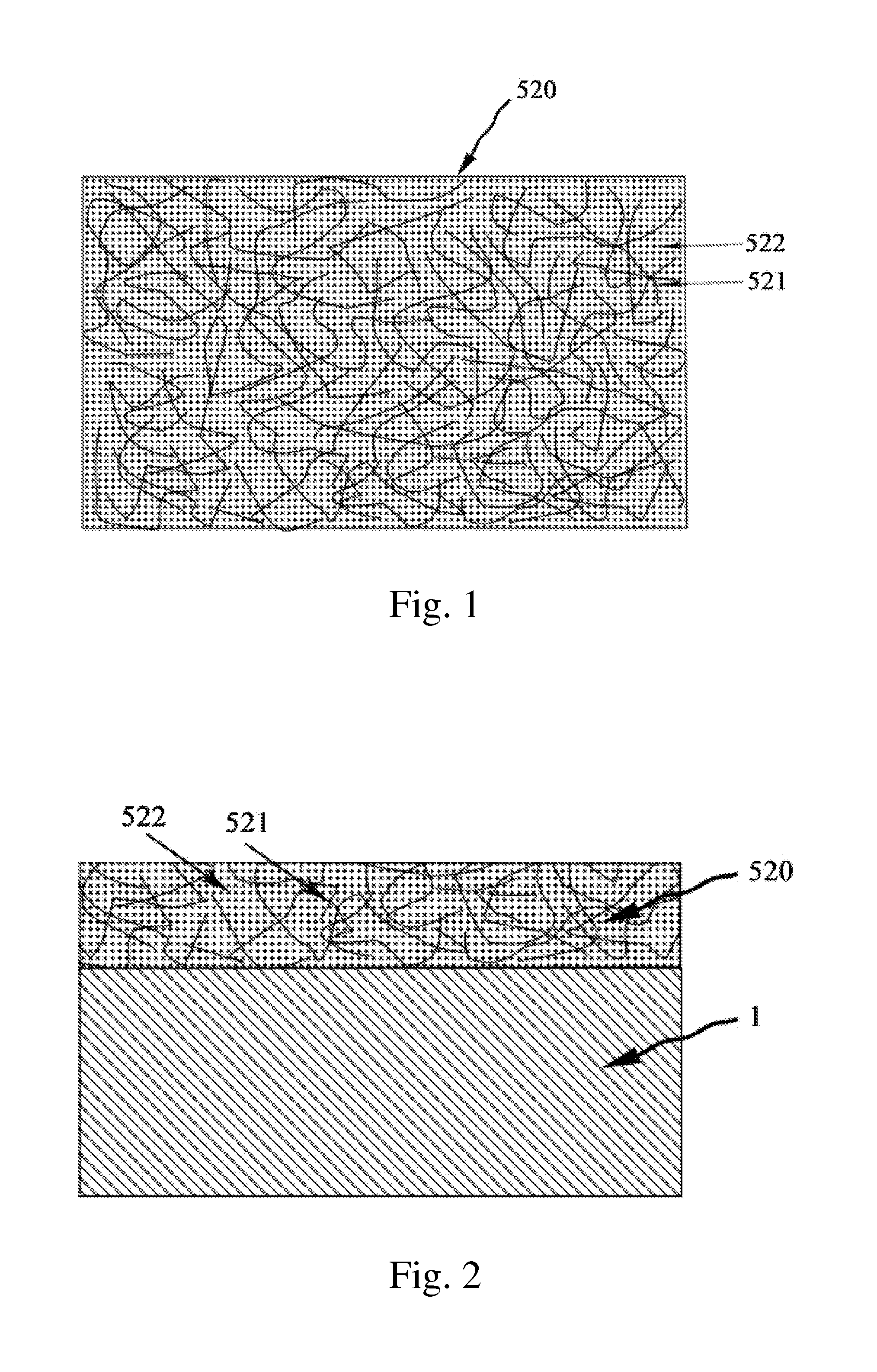
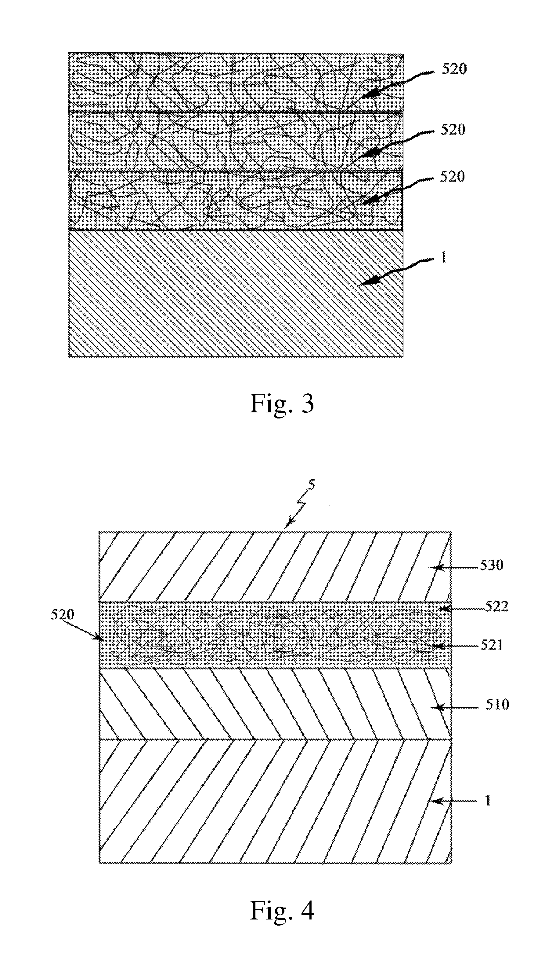
[0103]The guiding ideology of the present invention is to prepare the composite film with excellent comprehensive properties (as shown in FIG. 1) as the thermistor and light absorbing materials (as shown in FIGS. 5, 6 and 7) to improve the properties of the infrared or terahertz detectors using the respective excellent electrical and optical properties of the carbon nanotube and the vanadium oxide in the vanadium oxide-carbon nanotube composite film structure. The method for manufacturing the vanadium oxide-carbon nanotube composite film comprises the steps as follows. (1) Select the silicon wafer as the substrate 1 for growing the film thereon, firstly treat the silicon wafer by Piranha solution and clean the treated silicon wafer by deionized water, and th...


PUM


Abstract

A microbolometer includes a micro-bridge structure for uncooling infrared or terahertz detectors. The thermistor and light absorbing materials of the micro-bridge structure are the vanadium oxide-carbon nanotube composite film formed by one-dimensional carbon nanotubes and two-dimensional vanadium oxide film. The micro-bridge is a three-layer sandwich structure consisting of a layer of amorphous silicon nitride base film as the supporting and insulating layer of the micro-bridge, a layer or multi-layer of vanadium oxide-carbon nanotube composite film in the middle of the micro-bridge as the heat sensitive and light absorbing layer of the microbolometer, and a layer of amorphous silicon nitride top film as the stress control layer and passivation of the heat sensitive film. The microbolometer and method for manufacturing the same can overcome the shortcomings of the prior art, improve the performance of the device, reduce the cost of raw materials and is suitable for large-scale industrial production.

Description

BACKGROUND OF THE PRESENT INVENTION[0001]1. Field of Invention[0002]The present invention relates to uncooling infrared and terahertz detectors, and more particularly to a microbolometer and method for manufacturing the same.[0003]2. Description of Related Arts[0004]The infrared detector transforms the invisible infrared heat radiation into the detectable electrical signal to achieve the observation to the external affairs. There are two kinds of infrared detectors: the quantum detector and the thermal detector. The thermal detector is also known as the uncooling infrared detector which can be operated at the room temperature, and has some advantages of good stability, high integration and low price, and wide application prospect in the military, commercial and civil fields. The pyroelectric, thermocouple and thermal resistor are three main types of the uncooling infrared detector, wherein the microbolometer focal plane detector based on the thermal resistor is a rapidly developed u...

Claims


Application Information

Patent Timeline
IPC IPC(8): H01L31/101H01L31/18
CPCG01J5/02G01J5/023G01J5/20G01J5/046G01J5/04
Inventor XU, XIANGDONGJIANG, YADONG
Owner UNIV OF ELECTRONIC SCI & TECH OF CHINA
Why Eureka
Try Eureka