

Process for producing metallized substrate, and metallized substrate
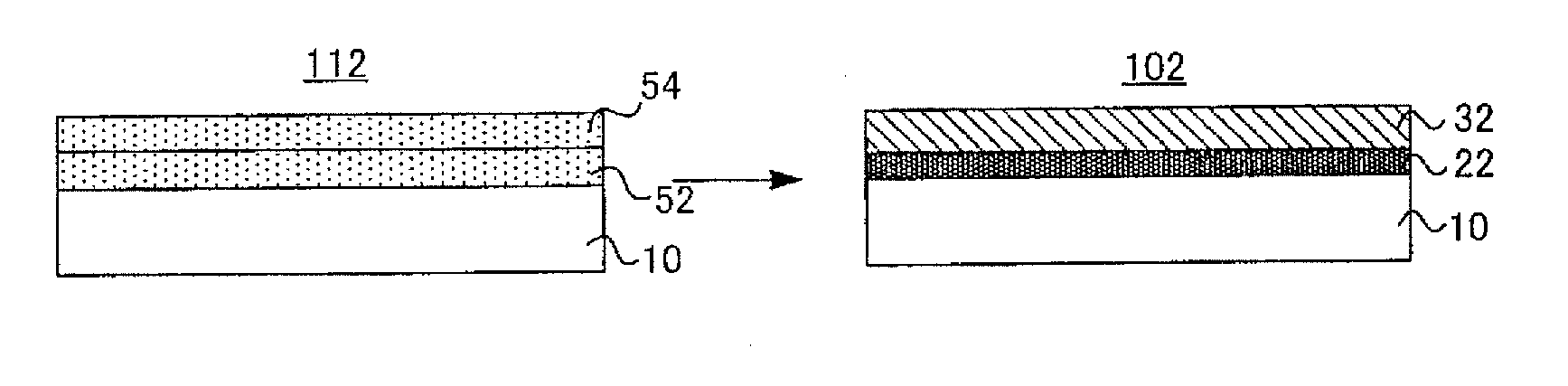
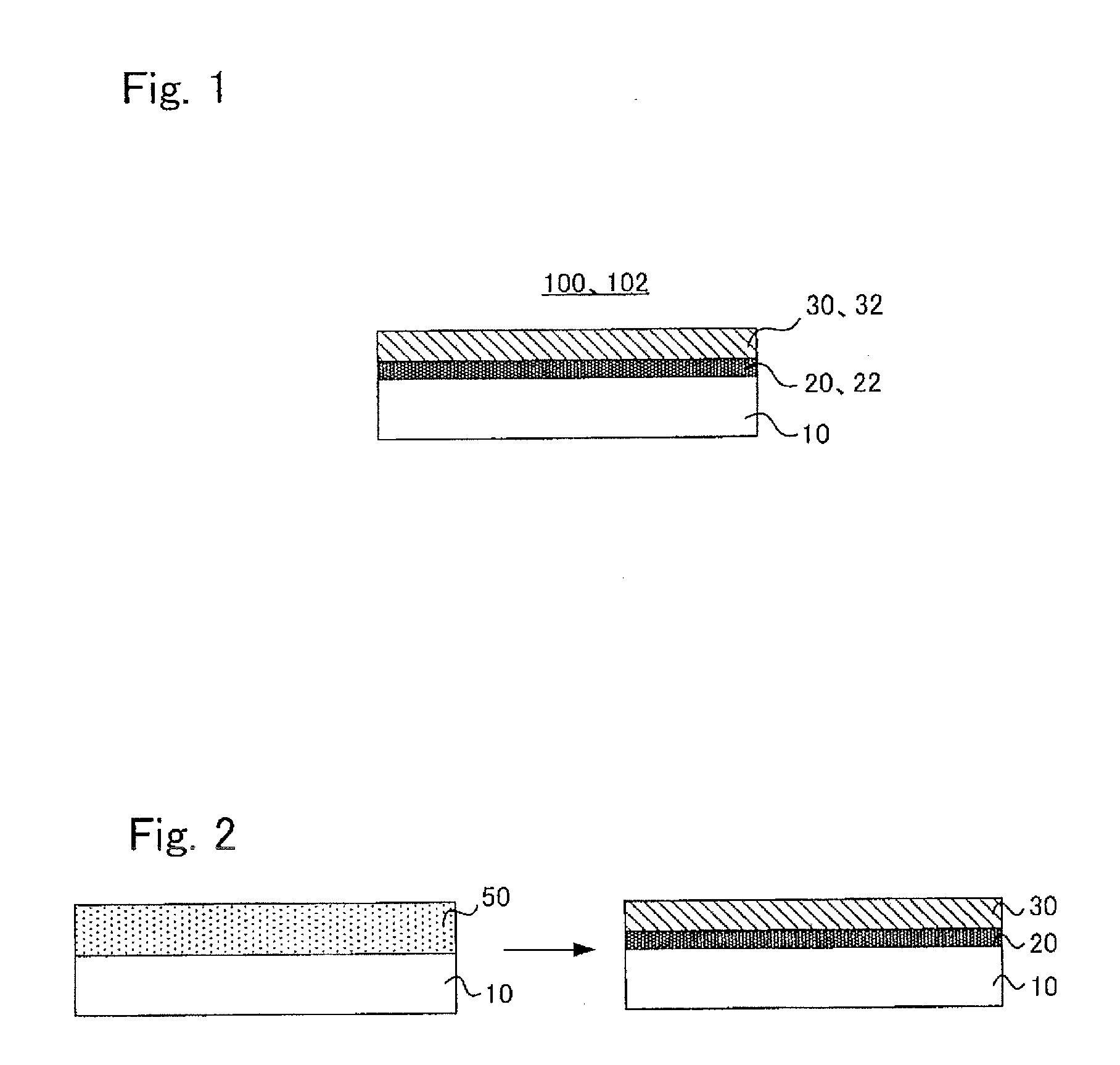
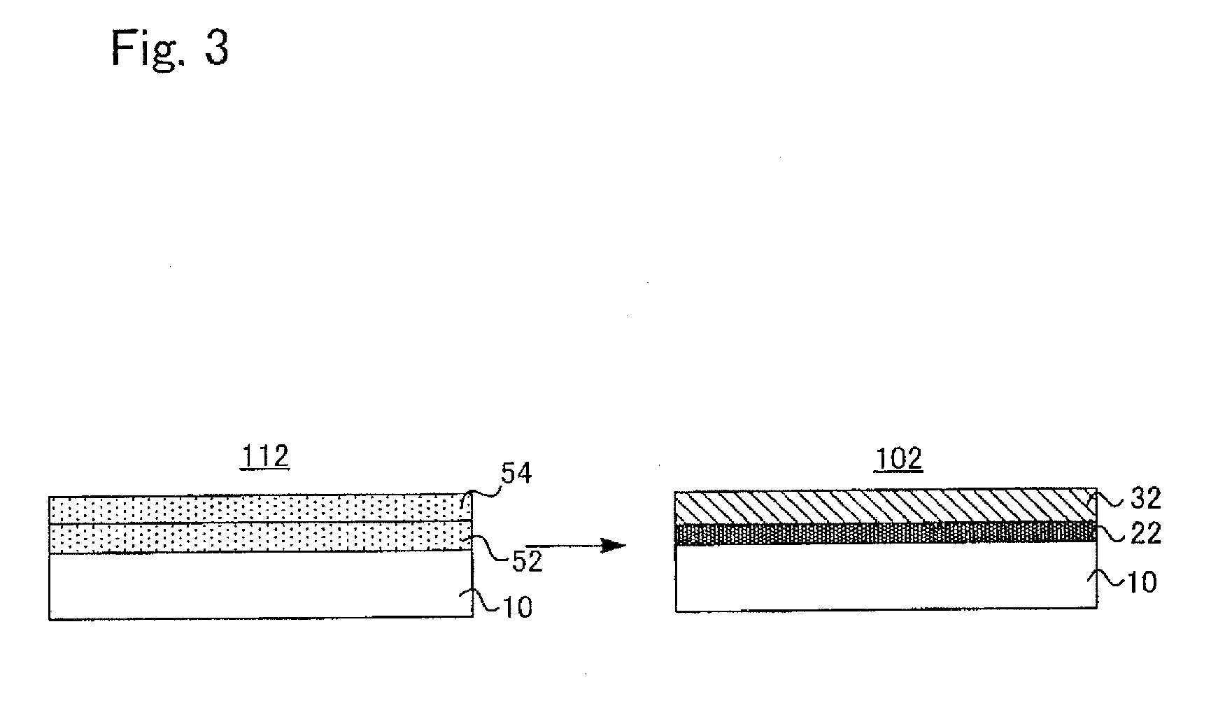
a technology of metallized substrates and metallized substrates, which is applied in the directions of liquid/solution decomposition chemical coating, semiconductor/solid-state device details, transportation and packaging, etc., can solve the problems of high resistance of wiring, high resistance of alumina sintered bodies, and high cost of noble metals such as au, so as to improve the metal-platability of the front surface, improve the resistance value of metal layers (30), and improve the electroconductivity of metal layers (30
- Summary
- Abstract
- Description
- Claims
- Application Information
AI Technical Summary
Benefits of technology
Problems solved by technology
Method used
Image

Examples
example 1
Production of a Paste Composition
[0128]A mortar was used to pre-mix 9 parts by mass of a copper powder having an average particle size of 0.3 μm (copper powder (b)), 91 parts by mass of a copper powder having an average particle size of 2 μm (copper powder (c)), 23 parts by mass of a silver powder (a) having an average particle size of 0.6 and 3.8 parts by mass of a titanium hydride powder having an average particle size of 5 μm with a vehicle in which poly(alkyl methacrylate) was dissolved in terpineol. Thereafter, a three-roll mill was used to subject the mixture to dispersing treatment to produce a metal paste composition.
[0129](Production of Metallized Substrate)
[0130]The produced metal paste composition was printed onto a sintered aluminum nitride substrate (trade name: “SH-30”, manufactured by Tokuyama Corp.), 0.64 μm in thickness, by screen printing, and then the resultant was dried at 100° C. for 10 minutes. Next, the workpiece was fired at 850° C. in a vacuum (vacuum degree...
examples 2 to 6
, and 9
[0147]Each metallized substrate was produced in the same way as in Example 1 except that the composition of the raw material of the paste was changed into a composition shown in Table 1, and then analyzed to be evaluated. The results are shown in Tables 1, 2 and 3.
example 7
[0148]A metallized substrate was produced in the same way as in Example 1 except that the composition of the raw material of the paste was changed into a composition shown in Table 1 and the firing temperature was changed to 900° C., and then analyzed to be evaluated. The results are shown in Tables 1, 2 and 3.
PUM
| Property | Measurement | Unit |
|---|---|---|
| thickness | aaaaa | aaaaa |
| thickness | aaaaa | aaaaa |
| particle size | aaaaa | aaaaa |
Abstract
Description
Claims
Application Information