
Temperature monitoring in a semiconductor device by using a pn junction based on silicon/germanium materials

a technology of temperature monitoring and silicon/germanium materials, applied in the field of integrated circuits, can solve the problems of increasing the power consumption of the entire device, increasing the power consumption of the mos circuit, and heat generation may reach extremely high values, so as to improve the temperature sensing capability of the semiconductor device, reduce the area consumption, and improve the effect of efficiency

Active Publication Date: 2012-02-02
ADVANCED MICRO DEVICES INC
View PDF1 Cites 3 Cited by
  • Summary
  • Abstract
  • Description
  • Claims
  • Application Information

AI Technical Summary

Benefits of technology

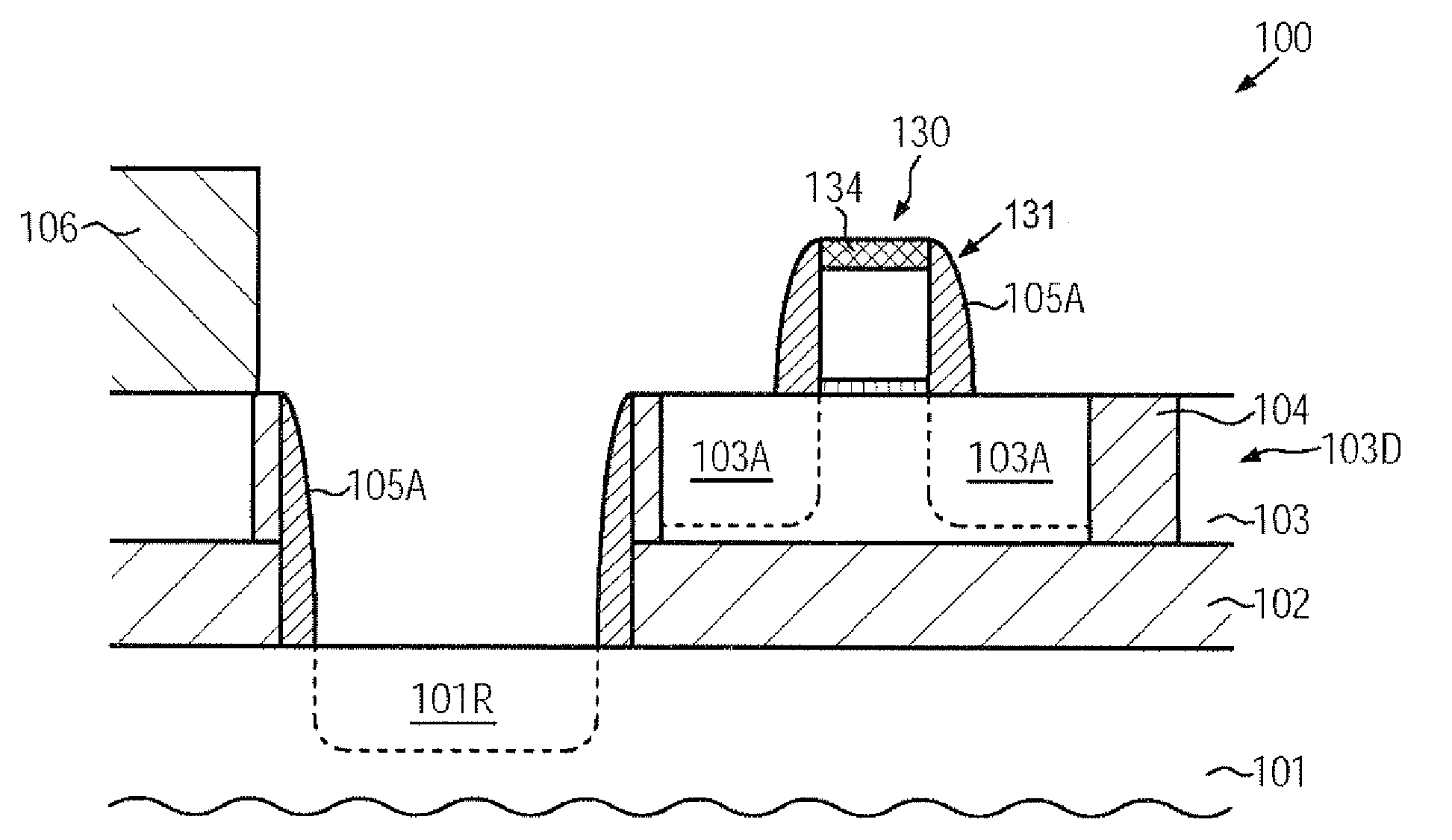
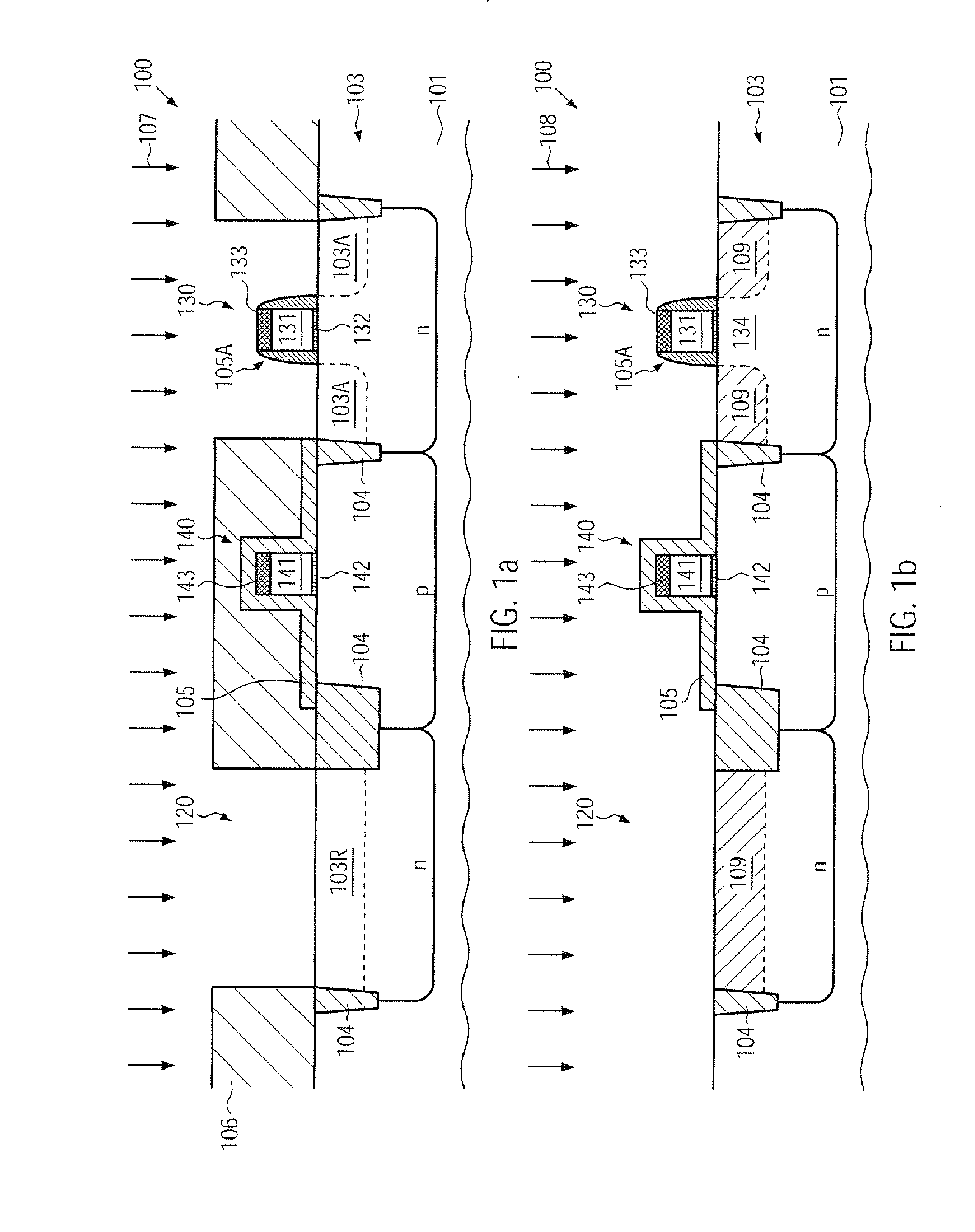
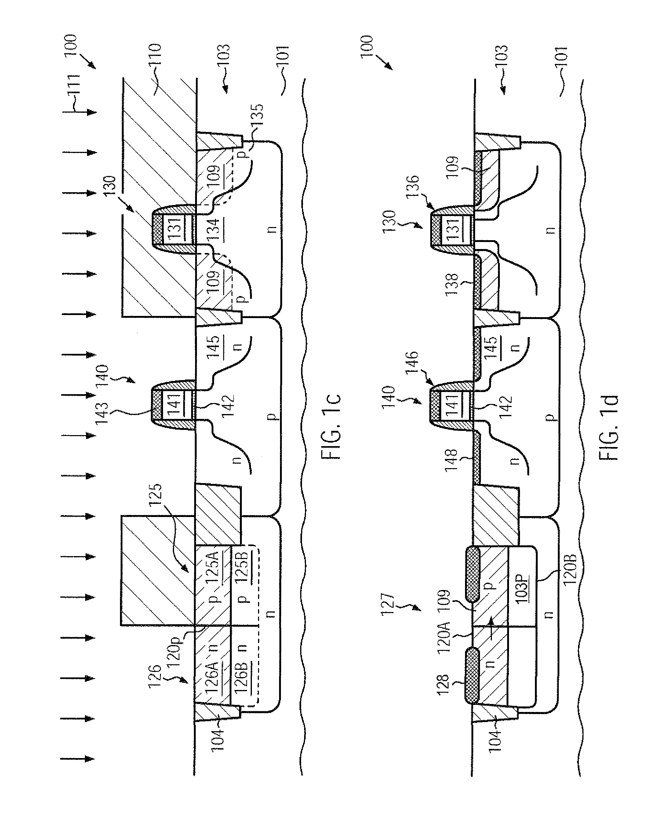
The patent text describes a method to enhance the temperature sensing capabilities of semiconductor devices by incorporating a semiconductor material with reduced band gap energy compared to silicon. This results in increased temperature sensitivity of diode structures, which can lead to reduced area consumption and higher efficiency for evaluating temperatures. The method can be used in semiconductor devices that use silicon-based materials, and it does not require additional process complexity. The increased temperature sensitivity can lead to better coverage of areas of interest within a die region, increasing the overall reliability of advanced semiconductor devices. The patent also describes a semiconductor device that includes a thermal sensing diode with enhanced temperature sensitivity. The method involves forming recesses in a silicon-containing crystalline semiconductor material and selectively growing a silicon / germanium alloy material in the recesses. The resulting diode structure has a PN junction formed by the P-doped region and the N-doped region, which can be used for estimating temperature.

Problems solved by technology

Furthermore, the reduced feature sizes may also be accompanied by reduced switching speeds of the individual transistors, thereby contributing to increased power consumption in MOS circuits, since the reduced switching speeds allow the operation of the transistors at higher switching frequencies, which in turn increases the power consumption of the entire device.
In sophisticated applications using densely packed integrated circuits, the heat generation may reach extremely high values due to the dynamic losses caused by the high operating frequency, in combination with a significant static power consumption of highly scaled transistor devices, owing to increased leakage currents that may stem from extremely thin gate dielectrics, short channel effects and the like.
Since external heat management systems may not enable a reliable estimation of the die-internal temperature distribution due to the delayed thermal response of the package of the semiconductor device and the possibly insufficient spatial temperature resolution, these external concepts may have to be designed so as to take into consideration these restrictions and provide sufficient operational margins with respect to heat control, or to risk otherwise overheating and thus possibly destruction of specific critical circuit portions.
The incorporation of a plurality of temperature-sensitive circuits, however, may result in a significant “consumption” of valuable real estate of the semiconductor die, which may typically cause a “competitive” situation during circuit design between actual circuit portions and temperature-sensitive areas.
Therefore, frequently, the temperature-sensitive circuit portions are treated with reduced priority compared to the “actual” circuit portions, which may finally result in a circuit design in which the temperature-sensitive circuits are positioned in less than ideal temperature sensing locations.
For instance, the design of performance-critical circuit portions of the device that may be operated at higher speed or frequencies may not be compatible with the provision of sensor elements in these critical areas, for example, due to undesired lengthening of the signal routing and reduction of speed.
Hence, although these performance-critical areas usually generate a significantly higher amount of heat, the temperature of such “hot spots” may not be reliably measured, since the temperature-sensitive circuits are positioned by the design constraints at distant locations.
Therefore, in this case, damage of the performance-critical areas may occur or respective heat management strategies may be required to take into account the discrepancy of the measurement data and the actual thermal conditions in the performance-critical areas.
Similarly, the thermal response of the temperature-sensitive circuits may be affected by the shielding effect of materials and structures that may be provided in the vicinity of the temperature-sensitive circuits.
For example, due to the reduced heat dissipation capability of semiconductor-on-insulator (SOI) devices caused by the buried insulating layer, on which the actual “active” device layer is formed, the corresponding sensing of the momentary temperature in SOI devices is of particular importance, wherein, additionally, the design-dependent positioning of the temperature sensitive circuits may further contribute to a less efficient overall temperature management in sophisticated SOI devices.
Thus, in addition to the shielding effect of the buried insulating layer, at least some additional process steps may be required, for instance, for etching through the semiconductor layer or a corresponding trench isolation area and through the buried insulating layer in order to expose the crystalline substrate material, thereby contributing to the overall process complexity.
Furthermore, the temperature-sensing diodes, in combination with an appropriate evaluation circuit, may also be subject to similar design constraints as described above, irrespective of whether a bulk architecture or an SOI architecture is considered.
Hence, currently employed die-internal temperature monitoring mechanisms, although providing significant advantages over external temperature management systems, may suffer from increased die area consumption due to low temperature sensitivity, possibly in combination with reduced proximity to hot spots, which may result in reduced reliability of the die-internal temperature control.

Method used


Image

  • Temperature monitoring in a semiconductor device by using a pn junction based on silicon/germanium materials
  • Temperature monitoring in a semiconductor device by using a pn junction based on silicon/germanium materials
  • Temperature monitoring in a semiconductor device by using a pn junction based on silicon/germanium materials

Examples


Embodiment Construction

[0025]Various illustrative embodiments are described below. In the interest of clarity, not all features of an actual implementation are described in this specification. It will of course be appreciated that in the development of any such actual embodiment, numerous implementation-specific decisions must be made to achieve the developers' specific goals, such as compliance with system-related and business-related constraints, which will vary from one implementation to another. Moreover, it will be appreciated that such a development effort might be complex and time-consuming, but would nevertheless be a routine undertaking for those of ordinary skill in the art having the benefit of this disclosure.

[0026]The present subject matter will now be described with reference to the attached figures. Various structures, systems and devices are schematically depicted in the drawings for purposes of explanation only and so as to not obscure the present disclosure with details that are well kno...


PUM

PropertyMeasurementUnit
concentrationaaaaaaaaaa
semiconductoraaaaaaaaaa
conductivityaaaaaaaaaa

Abstract

By incorporating germanium material into thermal sensing diode structures, the sensitivity thereof may be significantly increased. In some illustrative embodiments, the process for incorporating the germanium material may be performed with high compatibility with a process flow for incorporating a silicon / germanium material into P-channel transistors of sophisticated semiconductor devices. Hence, temperature control efficiency may be increased with reduced die area consumption.

Description

BACKGROUND[0001]1. Field of the Disclosure[0002]Generally, the present disclosure relates to the formation of integrated circuits, and, more particularly, to thermal sensing techniques in semiconductor devices on the basis of diode structures.[0003]2. Description of the Related Art[0004]The fabrication of integrated circuits requires a large number of circuit elements, such as transistors and the like, to be formed on a given chip area according to a specified circuit layout. Generally, a plurality of process technologies are currently practiced, wherein, for complex circuitry, such as microprocessors, storage chips, ASICs (application specific ICs) and the like, CMOS technology is currently one of the most promising approaches due to the superior characteristics in view of operating speed and / or power consumption and / or cost efficiency. During the fabrication of complex integrated circuits using CMOS technology, millions of complementary transistors, i.e., N-channel transistors and...

Claims


Application Information

Patent Timeline
Patent Type & Authority Applications(United States)
IPC IPC(8): H01L29/66H01L21/66
CPCH01L21/823807H01L27/1203H01L27/0629
Inventor STEPHAN, ROLFFORSBERG, MARKUSBURBACH, GERTMOWRY, ANTHONY
Owner ADVANCED MICRO DEVICES INC
Learn More