

Nanopore electrical sensor
a technology of electrical sensors and nanopores, applied in the field of sensor types, can solve the problem that the single-base resolution requirement of gene sequencing cannot be m
- Summary
- Abstract
- Description
- Claims
- Application Information
AI Technical Summary
Benefits of technology
Problems solved by technology
Method used
Image

Examples
embodiment 1
[0034]synthesis of graphene on Cu film by chemical vapor deposition (CVD) method may include the following steps. Prepare 1000 nm Cu film on SiO2 (300 nm) / Si (500 μm) substrate; load it into ultrahigh vacuum (5.0×10⁻⁹ ton); heat the Cu / SiO2 / Si at 950° C. for 30 min; form graphene on the Cu surface in C2H4 gas (˜10 Pa) environment for 10 min; and finally cool down the sample to room temperature quickly to obtain graphene film on the Cu film.
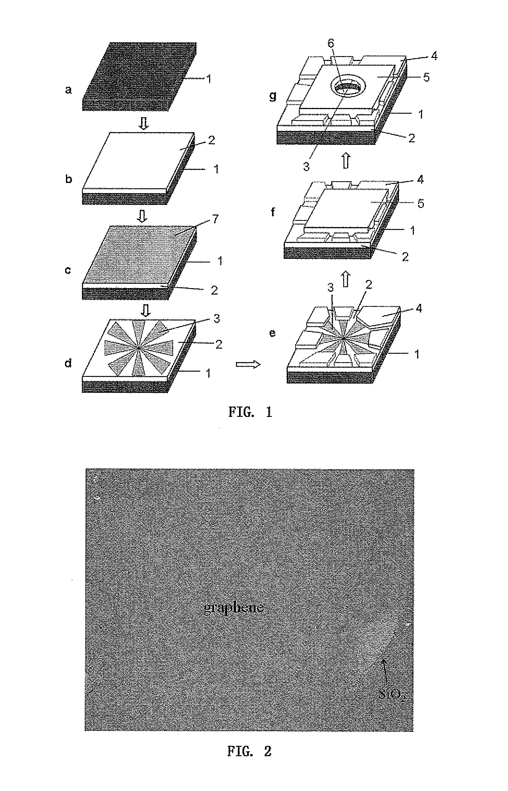
[0035]Referring to FIG. 1, FIG. 1 illustrates the process to prepare 100 nm SiO2 as the first insulating layer 2 (FIG. 1b) on single crystal silicon substrate 1 with thickness of 500 μm (FIG. 1a).
[0036]Transfer the synthesized graphene film onto the SiO2 / Si (FIG. 1c): spin-coat 500 nm polymethylmethacrylate (PMMA) on the synthesized graphene surface; put the PMMA / graphene / Cu into ferric nitrate solution to etch Cu layer away so as to obtain PMMA / graphene membrane; transfer the PMMA / graphene membrane onto the SiO2 / Si that is used to fabricate nanop...
embodiment 2
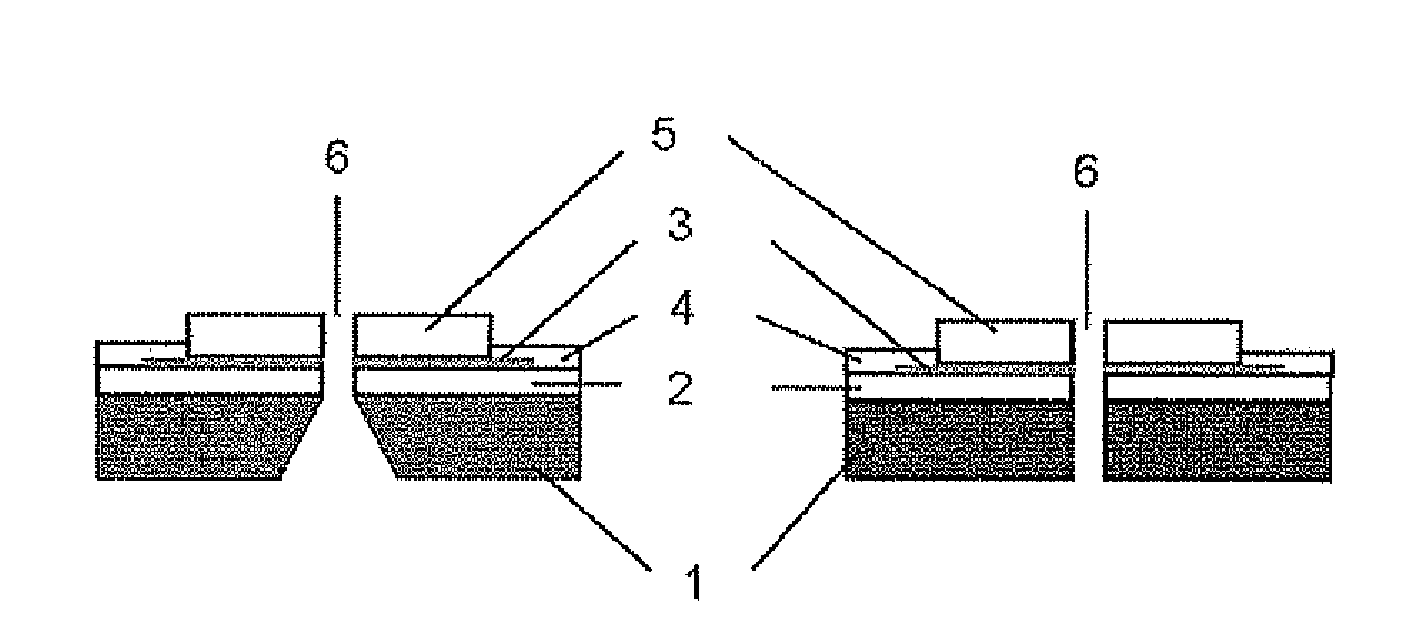
[0050]Referring to FIG. 4, load single crystal SiC{0001} substrate 1 with thickness of 500 μm into ultrahigh vacuum (1.0×10⁻¹° torr) for heat treatment (950° C.-1400° C.) to obtain the Si-terminated surface. The SiC substrate is also acted as the first insulating 2 (FIG. 4a). Such treatment leads to form epitaxial graphene layer as an electrode layer 7 (FIG. 4b). By using helium ion-beam etching technique, symmetrical electrode array 3 is patterned (FIG. 4c). Considering the thickness of graphene layer is 0.7 nm on the SiC, an electrical contact layer 4 consisting of Pd (50 nm) is prepared by photolithography and lift-off techniques (FIG. 4d). Then 100 nm Si3N4 serving as second insulating layer 5 (FIG. 4e) is prepared by low pressure CVD. Finally, a nanopore 6 with size of 3 nm (FIG. 4f, FIG. 6 and FIG. 7) is formed at the center of the radial-liked symmetrical electrode array 3.
[0051]Results and analysis: generally, insulating film material such as SiO2, Al2O3, HfO2, SiNx, BN, SiC...
embodiment 3
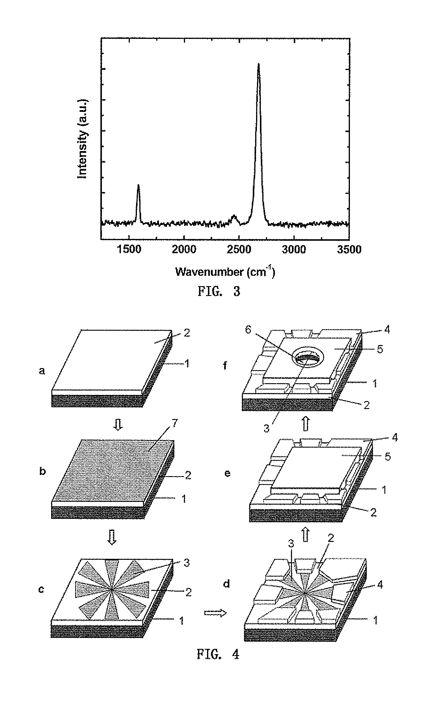
[0060]referring to FIG. 5, fabrication of nanopore electrical sensor may include the following steps: preparation of a combined layer of 100 nm SiO2 and 30 nm Si3N4 as the first insulating layer 2 (FIG. 5b) on a 600-μm-thick single crystal Si substrate 1 (FIG. 5a); formation of symmetrical-electrode-array-liked pattern of 100 nm Ni metal catalytic layer 8 (FIG. 5c) on the surface of Si3N4 first insulating layer 2 by using electron beam lithography and thermal evaporation techniques. The Ni pattern is used to synthesize graphene on it. Preferably, the synthesis of graphene layer on the patterned Ni layer 8 is as follows. Load the Ni / Si3N4 / SiO2 / Si into a ultrahigh vacuum (9×10⁻⁹ torr) chamber, and heat the structure at 950° C. for 30 min in CH4 (FIG. 5d) to form graphene layer on the Ni film. After that, the Ni layer is removed by using 1M FeCl3 solution, Consequently, the graphene layer with thickness of approx. 1.05 nm is automatically left on the Si3N4 / SiO2 first insulating layer 2...
PUM
| Property | Measurement | Unit |
|---|---|---|
| Thickness | aaaaa | aaaaa |
| Thickness | aaaaa | aaaaa |
| Thickness | aaaaa | aaaaa |
Abstract
Description
Claims
Application Information