Bipolar junction transistor

a bipolar junction transistor and transistor technology, applied in the field of bipolar junction transistors, can solve the problems of unavoidable small alignment errors, limited frequency at which the transistor can be switched between the on and off state, and other problems, to achieve the effect of improving the current gain of the device and reducing the current flow

Inactive Publication Date: 2012-03-15
SHARP KK
View PDF2 Cites 12 Cited by
  • Summary
  • Abstract
  • Description
  • Claims
  • Application Information

AI Technical Summary

Benefits of technology

[0031]An aspect of the invention is to employ base contact regions on one or both sides of a lateral BJT, and moreover to offset them towards the collector and / or sub collector using connecting base regions so that there is no direct contact, i.e. overlap, between the connecting base regions and the emitter. This greatly reduces the current flowing between the base and emitter when the junction is forward biased in normal operation, improving the current gain of the device.
[0039]The present invention overcomes the problems associated with the prior art as discussed above by virtue of the removal of direct contact, or overlap, between the connecting base regions and the emitter. This reduces the size of the forward biased p-n junction that exists between the emitter and the base and connecting base regions.
[0040]In common with JP H04-291926 this invention can be fabricated in a conventional TFT process flow without any additional complexity. A significant advantage over the prior art is the restriction on current flow between the base and emitter that this arrangement gives. A smaller base current results in a larger DC current gain and a more efficient device, giving improved performance for analogue applications.

Problems solved by technology

There will however always be unavoidable small errors in alignment, the magnitude of which depends on the accuracy of the mask aligner used.
Alternative substrate materials such as plastic have even more stringent maximum temperature limitations.
The frequency at which they can be switched between the on and off states is limited however.
Mass production requirements such as cost and yield limit the minimum achievable gate length and gate oxide thickness.
These factors, combined with the relatively low mobility of charge carriers in typical thin film semiconductors (e.g. amorphous Si, poly Si, metal oxide) mean that operating frequencies are generally limited to tens of MHz.
This can be problematic, since an AMLCD is typically expected to operate within a temperature range of −30° C. to 70° C. A bandgap reference circuit can help to overcome these difficulties by generating a reference voltage that is independent of temperature.
Unfortunately, the electrical properties of TFTs do not permit a simple implementation of a bandgap reference.
Firstly, the lack of a conductor-insulator-semiconductor gate stack results in the BJT having a much smaller capacitance than an equivalently sized MOSFET.
The main disadvantage of the BJT compared to the MOSFET is higher power consumption.
In contrast to the MOSFET, which typically only consumes a significant amount of power during switching between states, the BJT may consume power during the entire time that it is in the on-state.
This is due to the undesirable base current that flows in the device.
For this reason, it is generally not desirable to construct entire integrated circuits using only BJTs.
The major difficulty for BiCMOS circuitry is that it requires that MOSFETs and BJTs are fabricated together in a process flow.
Typically, this requires significantly more complex fabrication than is the case for a single device type, increasing cost.
In addition, the conduction carriers are not in close proximity to interfaces between materials, which typically degrade mobility and enhance the likelihood of recombination.
This makes the vertical BJT unsuitable for inclusion in a thin film process, in which the semiconductor thickness is typically less than 100 nm.
This structure retains many of the advantages of a vertical BJT, but would add a great degree of additional complexity and expense to a conventional TFT fabrication process, which only includes one semiconductor deposition step.
The disadvantage is that the regions must be positioned using lithography rather than controlling the depth of dopants with ion implantation or diffusion.
This makes it difficult to realise a short base, particularly since a contact to this region must be included for connecting to the base electrode 410.
However, this has the negative effect of increasing the base resistance, which degrades the high frequency performance.
Wide devices (10 μm or more) may have significantly degraded performance.
However, there are limits on how far the doping may be increased.
A highly doped base region thus creates a p-n junction in which both sides are highly doped, resulting in small depletion regions and large junction capacitance, which degrades high frequency performance.
Small depletion regions also give rise to large reverse junction leakage current and hot carrier degradation concerns, particularly for disordered films such as a-Si or poly-Si.
Both of these factors degrade the current gain of the device.
This is incompatible with device fabrication on a plastic or glass substrate.
However, the second base contact region does not completely remove the issue of non-linear collector current scaling with device width.
In this case it is the base region in the centre of the device that is least effective in controlling collector current.
This is due to the aforementioned problems that can arise when small depletion regions form between the base and collector, and increased junction capacitance.
A large junction of this type will result in a large current flowing between the base and emitter, degrading the current gain of the device.
Although the prior art therefore describes techniques for fabricating BJTs alongside MOSFETs, the majority of these are unsuitable for a thin film fabrication process without adding a large degree of complexity, or exceeding maximum temperatures for an AMLCD process.
This prior art device suffers from poor current gain however, due to large undesirable currents between the base and emitter.

Method used


Image

  • Bipolar junction transistor
  • Bipolar junction transistor
  • Bipolar junction transistor

Examples


first embodiment

[0111]the present invention provides a thin film lateral BJT with a single base contact region positioned in such a way as to minimise the current flow from base to emitter.

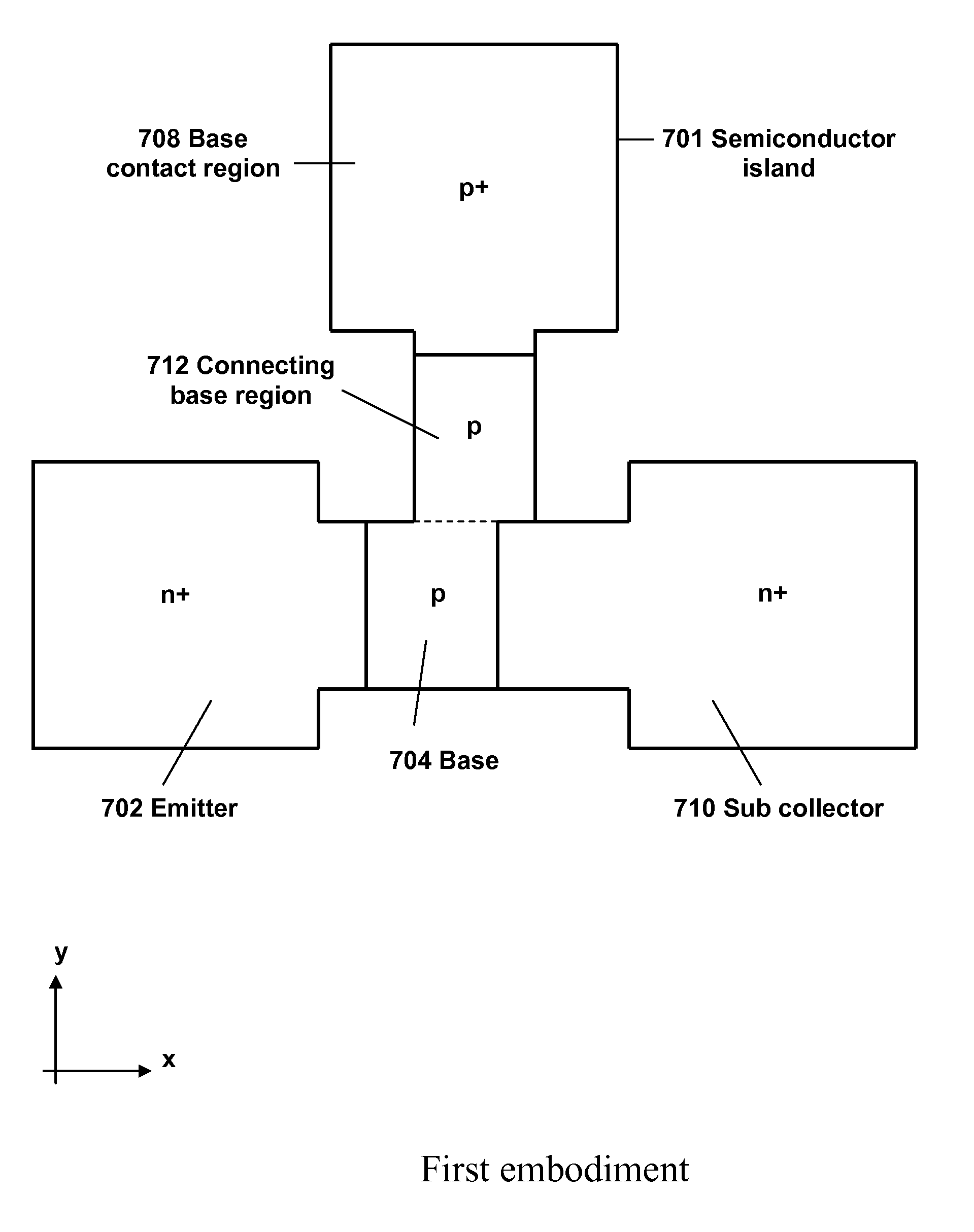
[0112]FIG. 7 illustrates the embodiment in plan view for the case of an npn BJT, but the invention applies equally to a pnp device. The BJT includes an island 701 of thin film semiconductor (most likely Si: either amorphous, polycrystalline or crystalline) positioned on top of an insulating substrate such as SiO2, SiNx on glass or plastic (not shown).

[0113]The semiconductor island 701 includes an emitter 702, base 704, base contact region 708, sub collector 710 and connecting base region 712. The emitter 702 and sub-collector 710 regions are heavily doped (approximately 1019-1021 cm−3) with a first conductivity type (e.g., n-type) and are separated by the base 704, which is doped with a second conductivity type (e.g., p-type). Typical n-type dopants for Si are arsenic or phosphor. Typical p-type dopants are boron...

third embodiment

[0118]In the invention, the BJT is formed as described in either of the first two embodiments, except that a collector 906 of the first conductivity type is positioned between the base 704 and sub collector 710 as shown in FIG. 9. The doping concentration of the collector 906 is less than that of the emitter 702 and sub collector 710, and may be less than, equal to, or greater than the concentration of either the base 704 or the base contact region(s) 708, 808. The collector 906 is likely to have a concentration in the range 1017-1019 cm−3. The connecting base region(s) 712, 812 contact(s) the base 704 and collector 906, but no longer contact(s) the sub collector 710.

[0119]This embodiment preserves the advantage resulting from the removal of the direct contact between the connecting base region(s) 712, 812 and the emitter 702. In addition, the reduced doping concentration of the collector 906 relative to the sub collector 710 results in reduced electric field strength in the base 70...

fourth embodiment

[0120]FIG. 10 illustrates the invention. In this embodiment, the BJT is formed as described in any of the first three embodiments, but the width of the sub collector 710 or collector 906 (if present) adjacent the base 704 is increased relative to the emitter 702. As will be appreciated, the width of the sub collector / collector and emitter is with reference to the direction perpendicular to the axis between the emitter and sub collector / collector (i.e., along the y-axis in FIG. 10).

[0121]This embodiment retains the advantages of previous embodiments, but the increased width of the collector 906 and / or sub collector 710 reduces the series resistance associated with this / these regions(s). The increased width improves the collection efficiency of charge carriers originating from the emitter 702. This increases the efficiency of the BJT and improves performance.

[0122]The BJT may be fabricated in a manner that is compatible with typical TFT fabrication processes. A thin film of semiconduc...


PUM


Abstract

A bipolar junction transistor includes a semiconductor island on an insulating substrate; an emitter and at least one of a collector and sub collector within the semiconductor island, the emitter and the at least one of the collector and the sub collector being of a first conductivity type; a base within the semiconductor island separating the emitter and the at least one of the collector and the sub collector, the base being of a second conductivity type; a base contact region within the semiconductor island, the base contact region being of the second conductivity type; and a connecting base region adjacent the base within the semiconductor island and connecting the base to the base contact region while not directly contacting the emitter, the connecting base region being of the second conductivity type with a doping concentration less than a doping concentration of the base contact region.

Description

TECHNICAL FIELD[0001]The present invention relates generally to bipolar junction transistors (BJTs), and more specifically to lateral bipolar junction transistors that may be fabricated in the manufacture of the display substrate of an active matrix liquid crystal display (AMLCD). Such lateral bipolar junction transistors enable analogue circuits, such as bandgap references or logarithmic converters that are difficult to achieve with thin film transistors (TFTs). The BJTs may also enable certain high frequency applications, such as RF communications.BACKGROUND ART[0002]FIG. 1 shows an AMLCD substrate 100. In the display pixel matrix 102, TFTs are located next to each pixel, or sub-pixel in the case of a colour display, to control the level of light emitted. TFTs are also widely used in the display gate and source drivers 104 and 106 respectively, and may also be employed in a sensor driver circuit 108. The AMLCD further includes a display controller 110 for providing appropriate con...

Claims


Application Information

Patent Timeline
Patent Type & Authority Applications(United States)
IPC IPC(8): H01L29/73
CPCH01L29/0821H01L29/7317H01L29/1008
Inventor NICHOLAS, GARETHHADWEN, BENJAMIN JAMESSHAH, SUNAY
Owner SHARP KK
Why Eureka
Try Eureka