Method for manufacturing semiconductor device

a manufacturing method and semiconductor technology, applied in semiconductor devices, capacitors, electrical devices, etc., can solve the problems of reducing the area on which a capacitor is formed, difficult to ensure the capacity required for a memory device, and the prospect of improving the features of a capacitor on the basis of these technical developments

Inactive Publication Date: 2012-03-15
ELPIDA MEMORY INC
View PDF2 Cites 310 Cited by
  • Summary
  • Abstract
  • Description
  • Claims
  • Application Information

AI Technical Summary

Benefits of technology

[0028]According to the present invention, since the uppermost layer of a dielectric film provided between a lower electrode and an upper electrode for a capacitor is formed at least by an atomic layer deposition (ALD) method and a protective film is formed on said dielectric film without exceeding the film forming temperature of the ALD method over 70° C., i.e., without imparting damages such as cracks to the dielectric film, the dielectric film can be free from damages such as cracks even if a heat treatment on film forming of the upper electrode, which has been formed on the protective film, is performed so that the capacitor can thus be formed with an excellent leakage current characteristic.

Problems solved by technology

As a result, the area on which a capacitor is formed decreases, and it is thus difficult to ensure the capacity required for a memory device.
Therefore, the prospect of improving the features of a capacitor on the basis of these technical developments is bleak.
However, it is well known that a dielectric film with high permittivity has small resistance to dielectric breakdown and has high leakage current.
However, a dielectric film composed of a single layer of zirconium oxide cannot achieve a sufficient thermostability, and leakage current likely increases after heat treatment.
However, the sputtering method may be used for a flat capacitor with no issue, but may not be applied for a three-dimensional capacitor because of inferior step coverage.
Furthermore, because the heated CVD method uses three kinds of source gases, uniformity in a film thickness or composite ratio may hardly be achieved as it goes down to the bottom of the deep holes in the three-dimensional structure.
However, the permittivity of SiN is twice as high as that of silicon oxide at best, and thus the whole capacitive insulation film would not substantially take advantage of the effect of using an STO film having a high permittivity.
In this capacitor structure, it is assumed that leakage current may be prohibited and reliability may be ensured, but a large capacity may not be obtained.
As paragraph of this document clearly mentions that the surface morphology of an STO film may deteriorate, the problem of an increase in leakage current would arise.
However, in the second embodiment, an electrode is formed directly on the STO film having a deteriorated surface morphology, and an increase in leakage current may not thus be avoided.

Method used


Image

  • Method for manufacturing semiconductor device
  • Method for manufacturing semiconductor device
  • Method for manufacturing semiconductor device

Examples


experiment 1

(Experiment 1)

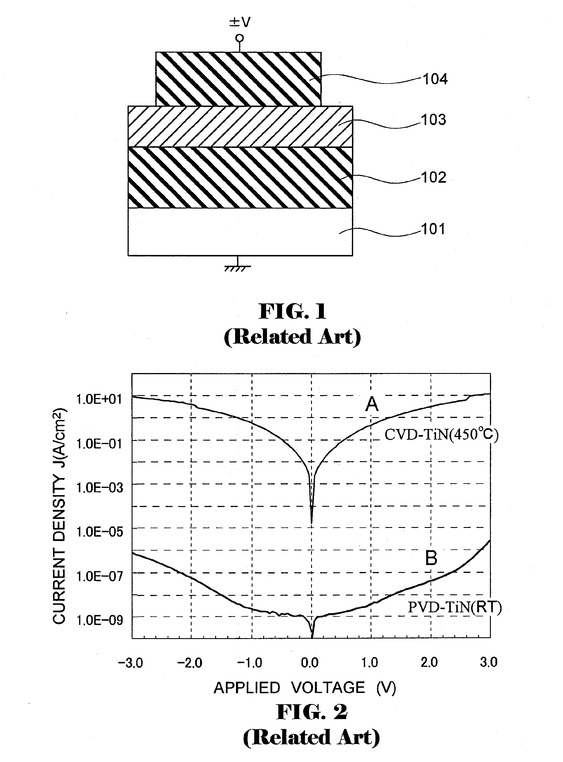
[0057]FIG. 1 shows the structure of a flat capacitor including, on semiconductor substrate 101, which is mono-crystalline silicon, lower electrode 102 made of a titanium nitride film (TiN film), upper electrode 104 made of a TiN film in the same way, and dielectric film 103 composed of a ZrO film sandwiched between the upper and lower electrodes.

[0058]Lower electrode 102 made of a TiN film has been formed using a chemical vapor deposition (CVD) method with reaction gases of titanium tetrachloride (TiCl4) and ammonia (NH3) in consideration of the application thereof to a three-dimensional structure. The deposition temperature was 450° C., and the thickness of the film was 10 nm. Hereinafter, a TiN film formed by a CVD method is referred to as a CVD-TiN film. The CVD-TiN film is a conductor in a polycrystalline state.

[0059]The ZrO film, which is to be dielectric film 103, has been formed using an atomic layer deposition (ALD) method with a reaction gas of ozone (O3) and ...

experiment 2

(Experiment 2)

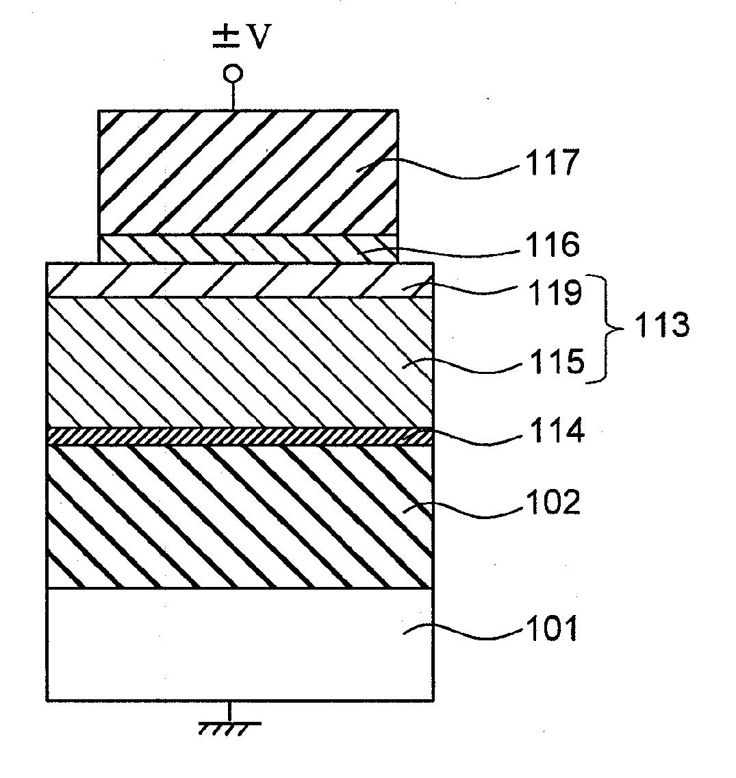
[0077]FIG. 6 illustrates a capacitor structure including, on mono-crystalline silicon semiconductor substrate 101, lower electrode 102 made of a CVD-TiN film, dielectric film 113 made of pc-ZrO film 113-c, first protective film 116 made of polycrystalline TiO (hereinafter referred to as “pc-TiO”) film 116-c, and upper electrode 117 made of a CVD-TiN film. The capacitor structure in this experiment is not three-dimensional semiconductor memory as explained above, and is constructed as a flat capacitor to achieve an easily manufacturable structure for evaluating its characteristics.

[0078]A method for manufacturing the capacitor depicted in FIG. 6 is now explained in reference to FIG. 7.

[0079]First, on semiconductor substrate 101, a CVD-TiN film, which is to be lower electrode 102, is formed by a CVD method with reaction gases of TiCl4 and NH3, as in Experiment 1, in consideration of its application to a three-dimensional structure. The film forming temperature can be 380...

experiment 3

(Experiment 3)

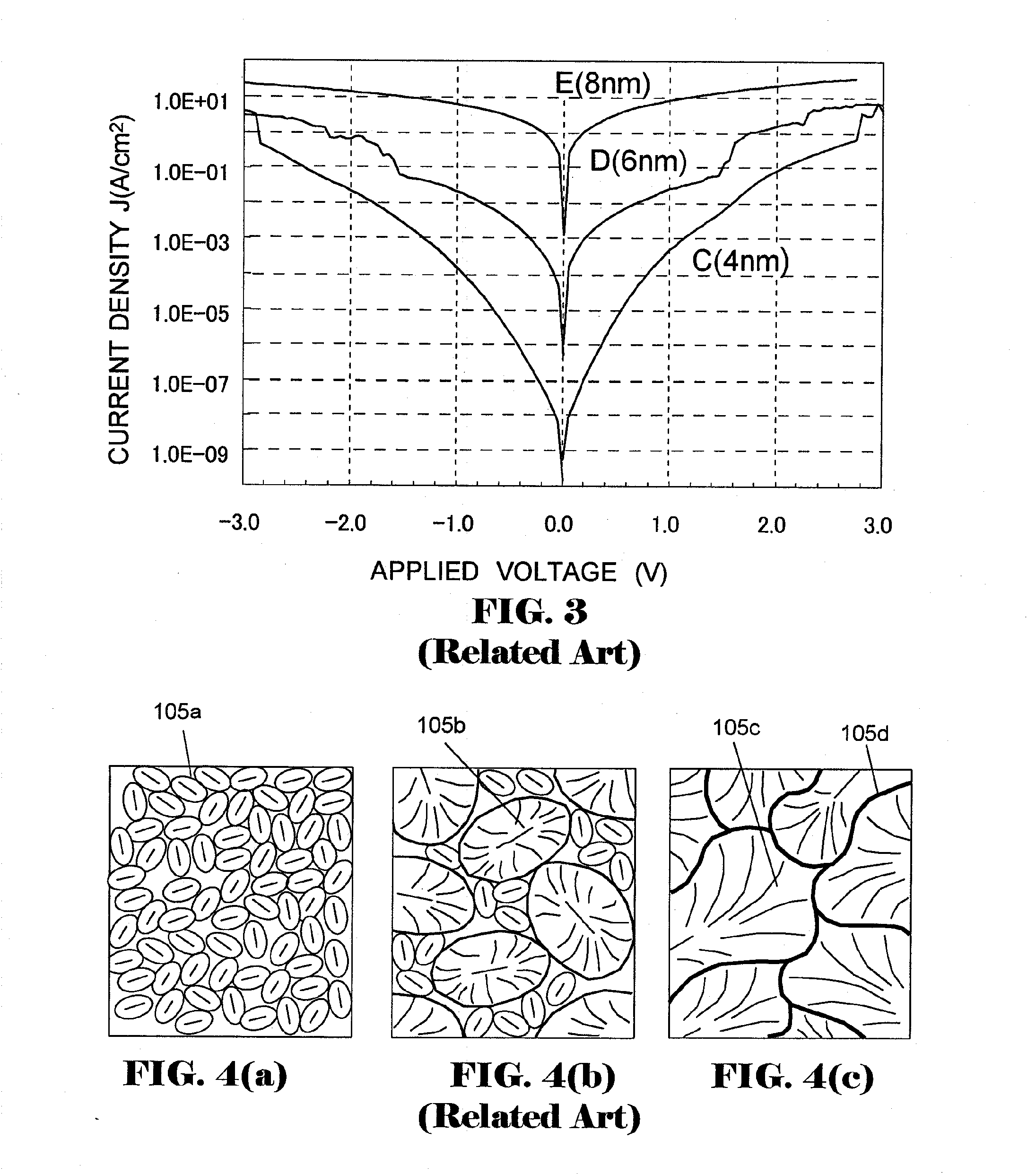
[0110]As explained in Experiment 2, a CVD-TiN film, which is to be upper electrode 117 in a capacitor including a ZrO film for the dielectric film, is formed at a temperature of 380° C. to 600° C. In this case, to avoid the cracks occurred with the secondary growth of crystal grains of the ZrO film, it is required to cover the surface of the dielectric film made of mc-ZrO film 113-a with first protective film 116 made of a-TiO film 116-a before forming upper electrode 117.

[0111]In this experiment, in order to improve further the leakage current characteristic, a capacitor structure in which, in addition to the aforementioned structure, a TiO film as a second protective film is formed between the lower electrode made of a TiN film and the ZrO film which is to be the dielectric film is described with reference to FIGS. 13 to 15. The capacitor according to this experiment has a stacked layer structure composed of a TiN film for upper electrode 117, a first TiO film for fi...


PUM

PropertyMeasurementUnit
temperatureaaaaaaaaaa

Abstract

A method for manufacturing a semiconductor device includes at least forming a lower electrode made of titanium nitride on a semiconductor substrate, forming a dielectric film comprising zirconium oxide, in which at least the uppermost layer of the dielectric film is formed by an atomic layer deposition (ALD) method on the lower electrode, forming a first protective film on the dielectric film without exceeding the film forming temperature of the ALD method over 70° C., and forming an upper electrode made of a titanium nitride on the first protective film.

Description

BACKGROUND OF THE INVENTION[0001]1. Field of Invention[0002]The present invention relates to a semiconductor device and a method of manufacturing the same, and, in particular, to dynamic random access memory (DRAM) having a capacitor with properties of low leakage current and high permittivity.[0003]2. Description of Related Arts[0004]DRAM has been used for a semiconductor memory operable at a high speed in a computer or other electronic devices. DRAM has a memory cell array and a peripheral circuit for operating the array. The memory cell array has a plurality of units arranged in a matrix, and each unit comprises one switching transistor and one capacitor.[0005]As in other semiconductor devices, DRAM has developed with miniaturization of each cell to satisfy a demand for high-integration. As a result, the area on which a capacitor is formed decreases, and it is thus difficult to ensure the capacity required for a memory device. To solve this problem, a three-dimensional structure ...

Claims


Application Information

Patent Timeline
Patent Type & Authority Applications(United States)
IPC IPC(8): H01L21/02
CPCH01L21/02189H01L21/0228H01L21/02304H01L21/02356H01L21/02362H01L28/75H01L27/10814H01L27/10852H01L27/10894H01L28/40H01L27/0207H10B12/315H10B12/09H10B12/033
Inventor HIROTA, TOSHIYUKIKIYOMURA, TAKAKAZU
Owner ELPIDA MEMORY INC
Why Eureka
Try Eureka