Material for organic electronics, organic electronic element, organic electroluminescent element, display element using organic electroluminescent element, illuminating device, and display device

a technology of electronic elements and materials, applied in the direction of thermoelectric device junction materials, conductive materials, solid-state devices, etc., can solve the problems of short service life of elements, difficult to eliminate water, and low light emission efficiency, and achieve stable driving for a long time, low temperature curing, and low voltage

Active Publication Date: 2012-07-19
RESONAC CORP
View PDF3 Cites 22 Cited by
  • Summary
  • Abstract
  • Description
  • Claims
  • Application Information

AI Technical Summary

Benefits of technology

[0073]According to the present invention, there can be provided a material for organic electronics which can produce an organic electronic element capable of lowering the driving voltage or capable of performing stable driving for a long time, and is capable of low temperature curing by a coating method; a multilayered organic electronic element using the material; an organic electroluminescent element; a display element; and an illuminating device. That is, when an ionic compound and a charge transporting compound are incorporated, an organic electronic element, particularly an organic EL element, which is capable of lowering of the driving voltage or capable of performing stable driving for a long time, can be obtained.
[0074]Furthermore, according to the present invention, an organic EL element having a multilayer structure can be obtained by a coating method, an organic EL element having excellent light emission efficiency or an excellent luminescence lifetime can be provided, and a display element, an illuminating device and a display device having those characteristics can be provided by using the organic EL element.

Problems solved by technology

Active research has been conducted hitherto on both the low molecular weight organic EL elements and the high molecular weight EL elements, but there are still serious problems of low light emission efficiency and short element service life.
The reason why multilayering is difficult in high molecular weight organic EL elements is that a lower layer which has been formed earlier is dissolved out at the time of the formation of an upper layer.
However, it is difficult to eliminate water, and this causes deterioration of the characteristics of the organic electronic element.
Furthermore, drying at a high temperature for a long time is required for the removal of water, so that production of an organic electronic element on a resin substrate becomes difficult, or restrictions are imposed on the process such as the pressure reduction conditions.
However, because the solvent that can be used in such a method is limited to a solvent which does not dissolve the lower layer, there is a problem that the selection range for the material is narrow.
In order to achieve sufficient insolubilization by this method, ultraviolet irradiation for a long time is required, and there is a problem that decomposition of triphenylamine and the like occurs.
In these methods, since a photoinitiator is used, there is a concern about deterioration by light.
Furthermore, sufficient insolubilization does not proceed at a low temperature, and there occurs a problem that the application of resin substrates which require low temperature curing is restricted, or a problem that at the time of the formation of an upper layer, the upper layer and the lower layer are mixed with each other, and the organic EL characteristics are deteriorated.
Moreover, the photoinitiators used in those methods are general iodonium salts or sulfonium salts, and there is a concern about the effect of the salts on the EL characteristics.

Method used


Image

  • Material for organic electronics, organic electronic element, organic electroluminescent element, display element using organic electroluminescent element, illuminating device, and display device
  • Material for organic electronics, organic electronic element, organic electroluminescent element, display element using organic electroluminescent element, illuminating device, and display device
  • Material for organic electronics, organic electronic element, organic electroluminescent element, display element using organic electroluminescent element, illuminating device, and display device

Examples


first embodiment

[Organic EL Element of First Embodiment]

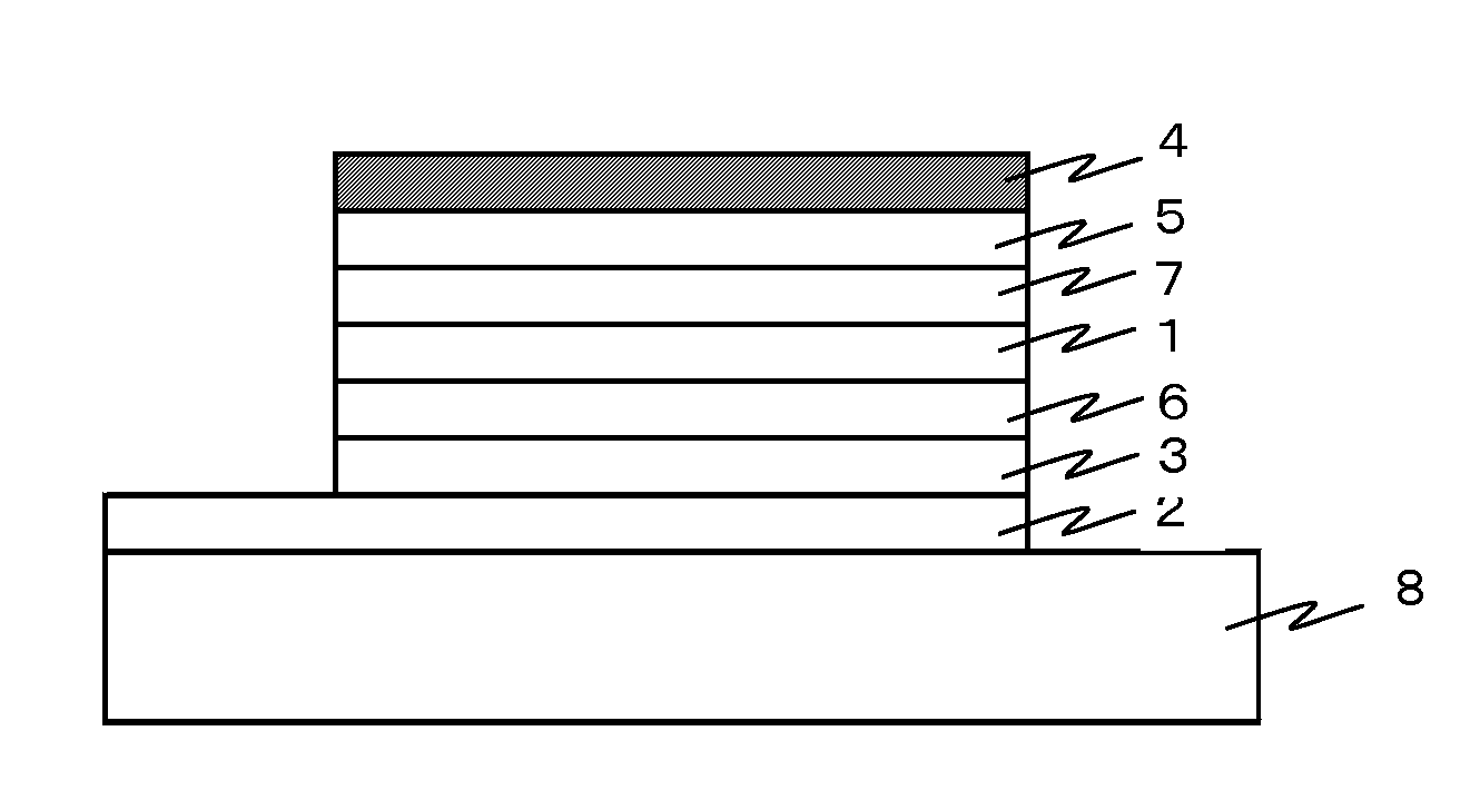
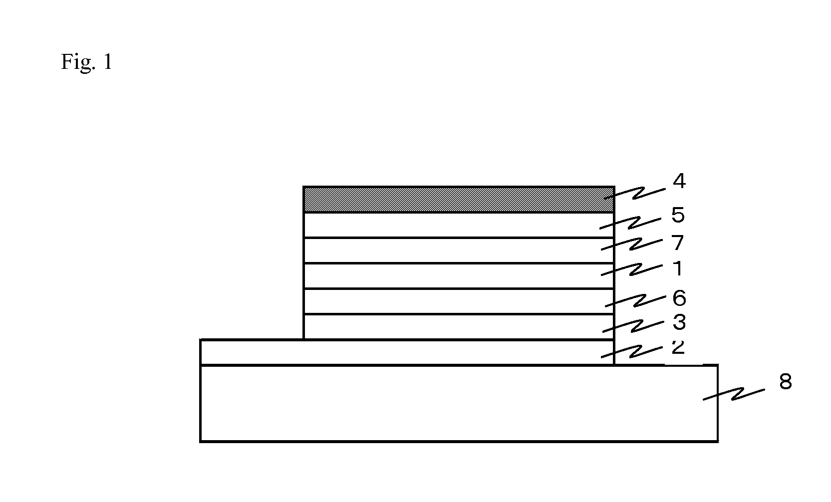
[0110]The organic EL element of the first embodiment of the present invention is characterized by having a layer formed from the material for organic electronics of the present invention as described above (hereinafter, also referred to as a polymerized layer). The organic EL element of the present invention is not particularly limited as long as it includes a light emitting layer, a polymerized layer, an anode, a cathode, and a substrate, and the organic EL element may also have other layers such as a hole injection layer, an electron injection layer, a hole transport layer, and an electron transport layer. The various layers will be explained in detail below.

[Light Emitting Layer]

[0111]The material used in the light emitting layer may be a low molecular weight compound, or may be a polymer or an oligomer, and a dendrimer or the like can also be used. Examples of a low molecular weight compound using fluorescent light emission include perylen...

second embodiment

[Organic EL Element of Second Embodiment]

[0136]The organic EL element of the second embodiment of the present invention has a multilayer structure, and is characterized in that two adjacent layers in the multilayer structure are formed by a coating method, respectively using a mixture containing a hole transporting compound having a polymerizable substituent, and the hole transporting compounds are respectively polymerized. Hereinafter, similarly to the first embodiment, a layer which is formed by a coating method using a mixture containing a hole transporting compound having a polymerizable substituent, and has the solubility modified by polymerizing the hole transporting compound, will be referred to as a polymerized layer.

[0137]The organic electroluminescent element of the second embodiment of the present invention has a multilayer structure, but the various layers in the multilayer structure are not particularly limited as long as the multilayer structure has a light emitting la...

example 1

(Evaluation of Polymerizability)

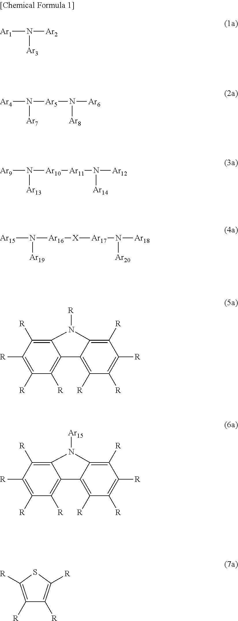
[0186]A coating solution prepared by mixing a toluene solution (400 μl) of a compound 1 (4.5 mg) shown below and an ethyl acetate solution (100 μl) of an ionic compound 1 (0.45 g) shown below, was spin coated on a quartz plate at 3000 rpm. Subsequently, the coated quartz plate was heated on a hot plate at 120° C. for 10 minutes to carry out a polymerization reaction. After the heating, the quartz plate was immersed for one minute in a solvent mixture of toluene:ethyl acetate (4:1), and was washed. The residual film ratio was measured from the ratio of the absorbances (Abs) of the maximum absorption (λmax) in the UV-vis spectrum obtained before and after washing.

[0187]Before washing: λmax=383 nm, Abs=0.229

[0188]After washing: λmax=383 nm, Abs=0.228

Residual film ratio(%)=Abs after washing / Abs before washing×100=0.228 / 0.229×100=99.6


PUM

PropertyMeasurementUnit
temperatureaaaaaaaaaa

Abstract

Provided is a material for organic electronics which can produce an organic electronic element capable of lowering the driving voltage or capable of performing stable driving for a long time. The material for organic electronics contains at least an ionic compound and a compound having a charge transporting unit (hereinafter, referred to as charge transporting compound), and the ionic compound is composed of a counter cation and a counter anion, while the counter cation is any one kind or two or more kinds selected from H+, a carbocation, a nitrogen cation, an oxygen cation, and a cation having a transition metal.

Description

TECHNICAL FIELD[0001]The present invention relates to a material for organic electronics, an organic electronic element using the material for organic electronics, an organic electroluminescent element (hereinafter, also referred to as an organic EL element), a display element using the organic electroluminescent element, an illuminating device, and a display device.BACKGROUND ART[0002]An organic electronic element is an element which performs an electrical operation using an organic substance, and is expected to exhibit features such as energy saving, low price, and flexibility. Thus, attention is being paid to the organic electronics as a technology to be substituted for the conventional inorganic semiconductors containing silicon as a main component.[0003]Among organic electronic elements, organic EL elements have attracted attention for their use in, for example, large-sized solid state light sources as the substitute for incandescent lamps and gas-filled lamps. Furthermore, org...

Claims


Application Information

Patent Timeline
Patent Type & Authority Applications(United States)
IPC IPC(8): H01L51/54B32B9/04H01B1/12
CPCC08G61/12H05B33/14C08G65/18C08G73/026C08G2261/1644C08G2261/3142C08G2261/3162C08G2261/3246C08G2261/342C08L63/00C09K11/06C09K2211/1433H01L51/0035H01L51/0039H01L51/0043H01L51/5056H01L51/5088C08G61/123H10K85/151H10K50/15H10K50/17H10K85/115H10K85/111
Inventor FUNYUU, SHIGEAKIISHITSUKA, KENICHIHOSHI, YOUSUKE
Owner RESONAC CORP
Why Eureka
Try Eureka