CMOS image sensor with non-contact structure
- Summary
- Abstract
- Description
- Claims
- Application Information
AI Technical Summary
Benefits of technology
Problems solved by technology
Method used
Image


Examples
Embodiment Construction
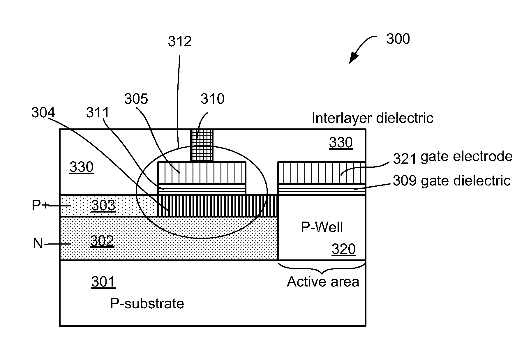
[0027]FIG. 3 illustrates a cross-sectional view of a CMOS image sensor device 300 according to an embodiment of the present invention. The CMOS image sensor device 300 includes a photodiode having an n− doped region 302 and a p+ doped region 303. The n-type doped region 302 may be defined by a mask and formed by implanting n-type dopants onto a region of a P-substrate 301. N-type dopants such as arsenic, antimony, or phosphorous may be employed. The P-type doped region 303 may be formed by conducting a masked implantation with p-type ions over the implanted n− region 302. P-type dopants such as boron, beryllium, indium, or magnesium may be employed. The doped regions 302 and 303 thus form a p-n photodiode that generates an electric charge when receiving an incident light. The CMOS image sensor further includes a capacitive coupling structure 312 that includes an n− doped region 304 as a bottom plate and a conductive layer 305 as a top plate. Capacitive coupling structure 312 also in...
PUM
 Abstract
Description
Claims
Application Information
 - R&D
- Intellectual Property
- Life Sciences
- Materials
- Tech Scout
- Unparalleled Data Quality
- Higher Quality Content
- 60% Fewer Hallucinations
Browse by: Latest US Patents, China's latest patents, Technical Efficacy Thesaurus, Application Domain, Technology Topic, Popular Technical Reports.
© 2025 PatSnap. All rights reserved.Legal|Privacy policy|Modern Slavery Act Transparency Statement|Sitemap|About US| Contact US: help@patsnap.com