Laminated structure for semiconductor devices

a semiconductor device and laminate technology, applied in the field of semiconductor devices, can solve the problems of device failure, limiting device durability, and fracturing of glass backplane substrates as dominant failure modes of current e-readers

Inactive Publication Date: 2012-11-08
CORNING INC
View PDF16 Cites 80 Cited by
  • Summary
  • Abstract
  • Description
  • Claims
  • Application Information

AI Technical Summary

Benefits of technology

[0009]One possibility is to use strengthened glass, such as Gorilla® (registered Trademark of Corning Incorporated) Glass as the backplane substrate. Ion-exchanged Gorilla® Glass, however, is sodium and potassium rich on the surface and alkali metal is a disadvantage in semiconductor device operation and fabrication, for example, TFT manufacturing. Free alkali metal ions can contaminate typical silicon (Si) TFT devices, and alkali containing glass is to be avoided in the typical high temperature vacuum p

Problems solved by technology

For those current products using glass as the backplane substrate, an impact with the floor, harsh environmental conditions, or similar event could cause device failure.
For example, fracturing of the glass backplane substrate is a dominant failure mode in current e-readers.
Glass is viewed by device manufacturers as limiting the device durability, and attempts have been made to replace it with other materials such as metal sheets (e.g. aluminum or stainless steel) and polymer films (polyethylene terephthalate or polyethylene naphthalate).
Although metal and polymer films are non-brittle,

Method used


Image

  • Laminated structure for semiconductor devices
  • Laminated structure for semiconductor devices
  • Laminated structure for semiconductor devices

Examples


example 1

Organic Bottom Gate, Top-Contact TFT on Ion-Exchange Glass

[0057]A TFT device can be fabricated by solution casting a thin layer of organic semiconducting materials such as thiophene copolymers onto a polymer dielectric layer.

[0058]This exemplary method comprises cleaning ion-exchanged glass substrates by using sonication in acetone and then isoproponol; depositing a patterned gold (Au) gate electrode at 2 Angstroms per second (Å / s) for 30 nm; spin-casting a mixture of 11 weight percent (wt %) (film thickness ˜800 nanometers (nm) to 1 um) poly vinyl-phenol (PVP) solution in Propylene Glycol Methyl Ether Acetate (PGMEA) and Melamine at 1000 rotations per minute (rpm) for 30 seconds (sec); and curing this layer by ultraviolet (UV)-light for less than 3 min. The method further comprises dissolving 3 milligrams per milliliter (mg / mL) of P2TDC17FT4 (organic semiconducting polymer) in 1,2-dichlorobenzene and spin-coating the solution; annealing the whole devices at 100° C. for 30 mins on a...

example 2

Bonding Flexible Glass Layer to an Ion-Eexchanged Glass Substrate and Fabricating a Transistor on the Flexible Glass Layer

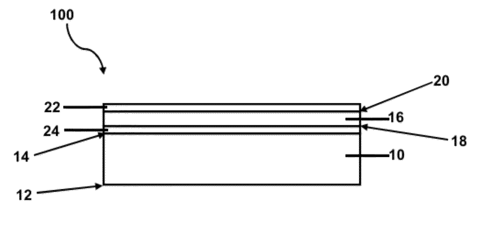
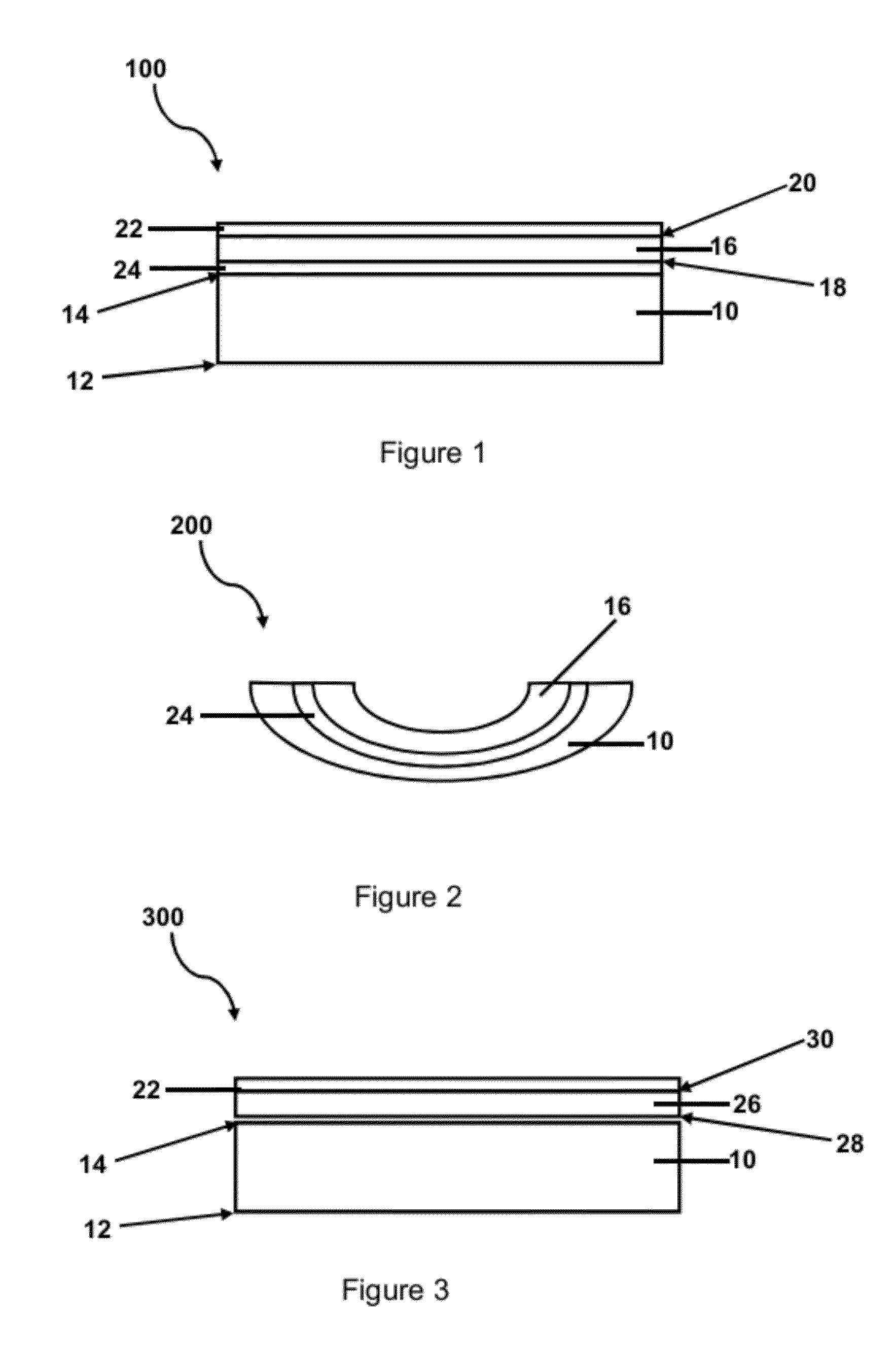
[0059]As mentioned previously, a flexible glass substrate can be bonded to a mechanically durable ion-exchanged glass substrate to produce a composite structure. This composite structure offers the alkali-free flexible glass surface for high quality TFT fabrication and performance. It also provides the high mechanical durability of the ion-exchanged glass.

[0060]The flexible glass layer can be made from an alkali-free glass composition and drawn to thicknesses of <300 um. For example, the flexible glass can have a thickness of 300 um or less, for example, 200 um or less, for example, 100 um or less, for example, 50 um or less. The flexible glass could have the dimensional tolerances and surface quality of typical fusion drawn LCD substrates to enable the fabrication of high performance TFT on its surface.

[0061]The ion-exchanged glass substrate can have a thickness...

example 3

Organic TFT Device Built on Flexible Glass Layers

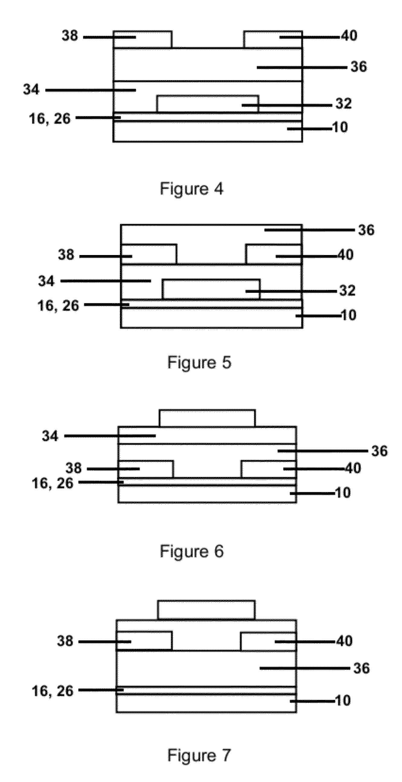
[0065]To demonstrate the ability of fabricating organic semiconductor devices on flexible glass, an organic TFT backplane was fabricated on 100 um thick flexible glass substrates. The fabrication of the OTFTs began with an organic hard coating which was spin-coated on the flexible glass as an adhesion promoter. The source and drain electrodes were formed by thermal-evaporated gold on the organic hard coating. The highly air-stable polymer semiconductor was then spin-coated and patterned by photolithography. A dielectric layer of 510 nm thick poly vinyl-phenol (PVP) was deposited and subsequently the gate electrode made of 50 nm gold metal was formed. Finally, 30 nm-thick organic interlayer film were spin-coated and the patterning of this film was done by photolithography again. Note that the via-holes through the interlayer and the dielectric to drain electrode were done by inductively coupled plasma reactive ion etcher. When fabricat...


PUM

PropertyMeasurementUnit
Lengthaaaaaaaaaa
Forceaaaaaaaaaa
Depthaaaaaaaaaa

Abstract

Articles are described utilizing laminated glass substrates, for example, ion-exchanged glass substrates, with flexible glass or polymers and with semiconductor devices which may be sensitive to alkali migration are described along with methods for making the articles.

Description

[0001]This application claims the benefit of priority under 35 U.S.C. §120 of U.S. Application Ser. No. 61 / 483175 filed on May 6, 2011 the content of which is relied upon and incorporated herein by reference in its entirety.BACKGROUND[0002]1. Field[0003]Embodiments relate generally to articles using laminated structures and more particularly to semiconductor devices using strengthened glass as backplane substrates with flexible glass layers or polymer layers and methods of making the same.[0004]2. Technical Background[0005]As semiconductor devices, such as e-readers, display devices, photovoltaic devices, thin-film transistors (TFTs) and other electronic gadgetry continue to gain worldwide acceptance, the demand for higher device mechanical durability grows. For those current products using glass as the backplane substrate, an impact with the floor, harsh environmental conditions, or similar event could cause device failure. For example, fracturing of the glass backplane substrate i...

Claims


Application Information

Patent Timeline
IPC IPC(8): H01L29/02H01L21/20B32B17/00
CPCB32B17/10018B32B17/10036B32B17/10119B32B17/10137Y02E10/549G02F2001/133302H01L51/0097H01L51/0512B32B2367/00G02F1/133302B32B1/00B32B17/06B32B2457/20B32B2457/12H10K10/462H10K77/111
Inventor GARNER, SEAN MATTHEWHE, MINGQIANLAHIRI, JOYDEEPLI, JIANFENGSORENSEN, MICHAEL LESLEYWEEKS, WENDELL P.
Owner CORNING INC
Why Eureka
Try Eureka