Silicon wafers by epitaxial deposition

a technology of silicon wafers and epitaxial deposition, which is applied in the direction of specific components, crystal growth process, polycrystalline material growth, etc., can solve the problems of high cost of silicon wafer manufacturing, and insufficient evidence of cost advantages of most thin film processes. achieve the effect of reducing silicon usage and production cost, high efficiency and reducing manufacturing costs of single crystals

Inactive Publication Date: 2013-02-07
SVAGOS TECHNICK INC
View PDF0 Cites 20 Cited by
  • Summary
  • Abstract
  • Description
  • Claims
  • Application Information

AI Technical Summary

Benefits of technology

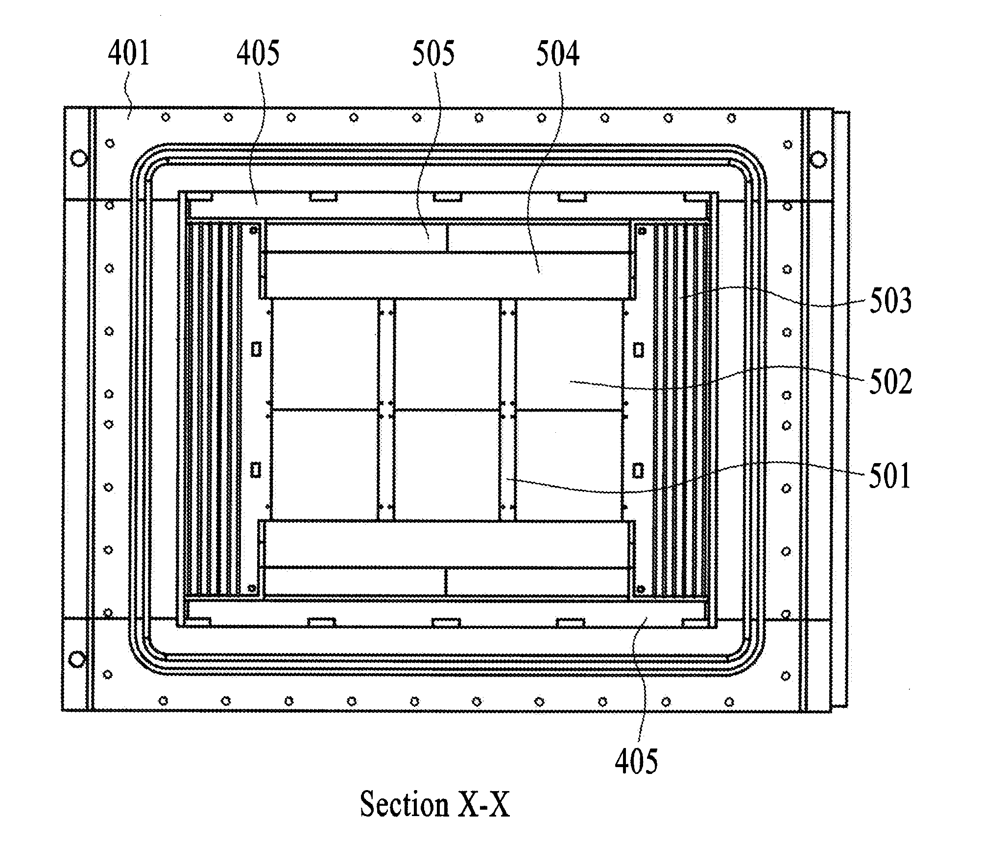
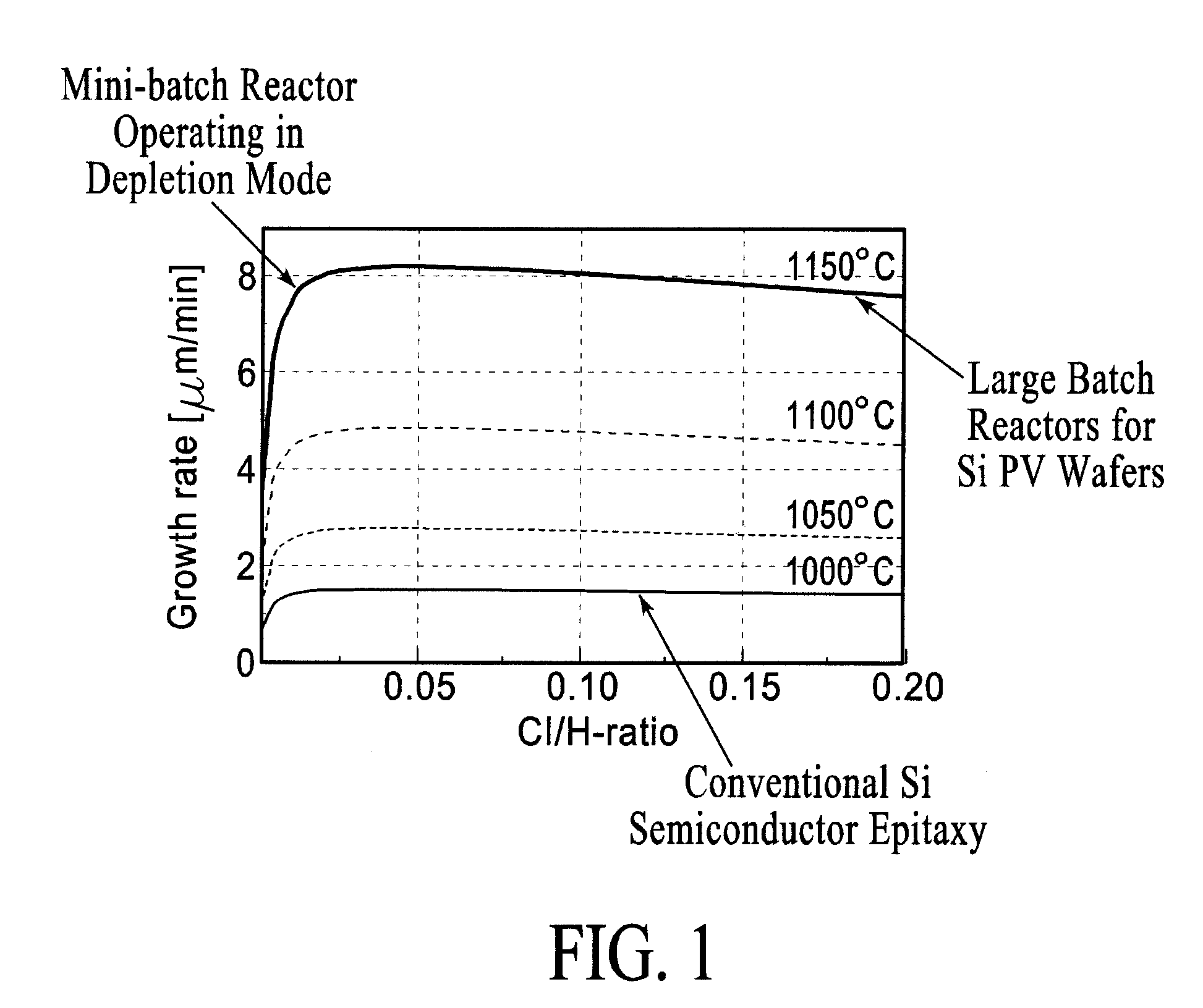
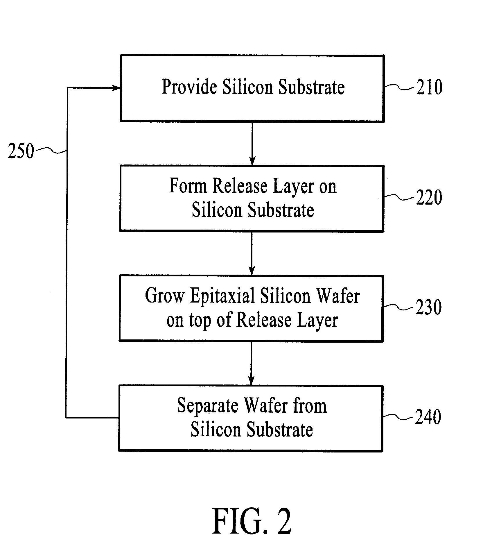
[0026]The present invention as described herein is a transformative technology for the reduction of manufacturing costs of single crystal silicon photo-voltaics based on the method involving direct-epitaxial deposition of the silicon wafers. Monocrystalline silicon wafers are produced directly from the gas phase, using technology that bypasses the steps of (a) polysilicon production, (b) crystal growth, and (c) wafering of the ingots. This enables a substantial reduction in silicon usage and production cost with a potential for manufacturing costs approaching grid parity for high efficiency PV modules. Key innovations in process and equipment technologies, which alone or in combination, enable stringent cost and technology targets, as well as scalability into volume production, include: epitaxial deposition in a silicon precursor depletion mode with cross-flow deposition to compensate for the decrease in silicon deposition rate on substrates along the direction of gas flow; a deposition system comprising multiple mini-batch reactors; a substrate carrier with low total heat capacity, high emissivity and small volume; a lamp module with rapid heat-up, efficient heat production, and spatial control over heating; and a manifold designed for cross-flow processing. Furthermore, the substrate carrier may include heat reflectors to control heat loss from the edges of the carrier and / or heat chokes to thermally isolate the carrier from the manifolds, allowing independent temperature control of the manifolds. The carrier and substrates may be configured for deposition on both sides of the substrates—the substrates having release layers on both sides and the carriers configured to have equal process gas flow over both surfaces of the substrate. Furthermore, the deposition system may be configured to allow removal of substrate carriers from the reactor while the substrate carrier is still at 400 to 600° C., thus reducing process cycle time through the reactor. Furthermore, the substrate carrier may be configured to engage with the gas manifold in the reaction chamber of the reactor to contain process gases within the substrate carrier, thus enabling a low frequency of cleaning for the reaction chamber of the reactor and a high reactor availability.

Problems solved by technology

However, crystalline silicon traditionally has a higher photovoltaic module cost than competitive thin-film panels.
A large part of this cost comes from the cost of manufacturing the silicon wafers (currently ˜180 μm thick), which includes the cost of polysilicon production, ingot formation, and wafering (wire sawing the ingot and finishing the cut wafers).
However, in general thin film photovoltaic (PV) modules typically have efficiencies substantially less than that of crystalline silicon modules.
In addition, the cost advantages of most thin film processes have not been conclusively demonstrated.
PV cell and module costs are approaching asymptotic levels with the deployment of large scale production equipment and single crystal silicon cell efficiencies near 19% have been reached, and further increases in cell efficiency may only be achieved at increased cost.
Similarly, a continuous Czochralski crystal growth process may provide incremental cost improvements, but radical cost reductions are unlikely.
However, sawing wafers to less than 180 μm has been plagued by lower yields and disproportionately higher kerf losses, as the wire saw technology starts to reach fundamental mechanical limits.
In fact, the capital costs—the one-time set-up costs for manufacturing—for polysilicon, ingoting and wafering dominate the total capital costs for production of silicon PV devices.
However, the challenge is utilizing an epitaxial deposition process at a cost which is comparable if not lower than traditional processes for manufacturing the single crystal silicon wafers.
However, high temperature processing of single wafers is cost prohibitive for all except the very high value devices such as cutting edge processors.
However, having to rotate the wafers limits reactor types to either single wafer reactors or small batch reactors.
Although higher growth rates can be achieved in these reactors, design constraints due to the requirement for wafer rotation at deposition temperatures generally keeps the operating temperature in the 1,000 to 1,050° C. range.
Fourth, the substrates must be heated-up to deposition temperature and then cooled-down after deposition is complete—this typically takes one hour and is on top of the deposition time for throughput calculations if done in the deposition chamber.
However, using commercial semiconductor epitaxial reactors it is estimated to cost substantially more than this—roughly $16.6 per wafer.

Method used


Image

  • Silicon wafers by epitaxial deposition
  • Silicon wafers by epitaxial deposition
  • Silicon wafers by epitaxial deposition

Examples


Embodiment Construction

[0053]Embodiments of the present invention will now be described in detail with reference to the drawings, which are provided as illustrative examples of the invention so as to enable those skilled in the art to practice the invention. Notably, the figures and examples below are not meant to limit the scope of the present invention to a single embodiment, but other embodiments are possible by way of interchange of some or all of the described or illustrated elements. Moreover, where certain elements of the present invention can be partially or fully implemented using known components, only those portions of such known components that are necessary for an understanding of the present invention will be described, and detailed descriptions of other portions of such known components will be omitted so as not to obscure the invention. In the present specification, an embodiment showing a singular component should not be considered limiting; rather, the invention is intended to encompass ...


PUM

PropertyMeasurementUnit
thickaaaaaaaaaa
operating temperatureaaaaaaaaaa
temperatureaaaaaaaaaa

Abstract

A system for depositing thin single crystal silicon wafers by epitaxial deposition in a silicon precursor depletion mode with cross-flow deposition may include: a substrate carrier with low total heat capacity, high emissivity and small volume; a lamp module with rapid heat-up, efficient heat production, and spatial control over heating; and a manifold designed for cross-flow processing. Furthermore, the substrate carrier may include heat reflectors to control heat loss from the edges of the carrier and/or heat chokes to thermally isolate the carrier from the manifolds, allowing independent temperature control of the manifolds. The carrier and substrates may be configured for deposition on both sides of the substrates—the substrates having release layers on both sides and the carriers being configured to have equal process gas flow over both surfaces of the substrate. High volume may be addressed by a deposition system comprising multiple mini-batch reactors.

Description

CROSS-REFERENCE TO RELATED APPLICATIONS[0001]This application claims the benefit of U.S. Provisional Application No. 61 / 491,152 filed May 27, 2011, incorporated herein by reference in its entirety.FIELD OF THE INVENTION[0002]The present invention relates generally to fabrication of silicon wafers, and more particularly to fabrication of silicon wafers by epitaxial deposition.BACKGROUND[0003]Crystalline silicon provides high solar cell efficiencies, η, of up to approximately 23% in commercial production environments, together with advantages, when compared with thin film solar cells such as CIGS, CdTe, etc., of (a) availability, (b) environmentally friendliness, and (c) demonstrated long lifetimes and associated technology maturity. However, crystalline silicon traditionally has a higher photovoltaic module cost than competitive thin-film panels. (A module is the unit that actually generates power and includes a frame holding a number of solar cells, the latter being electrically con...

Claims


Application Information

Patent Timeline
Patent Type & Authority Applications(United States)
IPC IPC(8): C30B25/14C30B25/12
CPCH01L21/02381H01L21/0245H01L21/02513C30B29/06H01L21/0262C30B25/165H01L21/02532C30B25/105C30B25/12C30B25/14C30B25/20Y02E10/547H01L21/20H01L21/324H01L21/683H03K19/195H01L31/1804
Inventor SIVARAMAKRISHNAN, VISWESWARENRAVI, TIRUNELVELI S.KASZUBA, ANDRZEJTRUONG, QUOC VINHVATUS, JEAN R.
Owner SVAGOS TECHNICK INC
Why Eureka
Try Eureka