Multijunction hybrid solar cell incorporating vertically-aligned silicon nanowires with thin films

a solar cell and nanowire technology, applied in the field of photovoltaic devices, can solve the problems of high production cost, high production cost, and severely limited applicability of such solar cells, and achieve the effects of enhancing photon absorption, reducing contact resistance, and high efficiency

Inactive Publication Date: 2013-04-04
UT BATTELLE LLC
View PDF5 Cites 11 Cited by
  • Summary
  • Abstract
  • Description
  • Claims
  • Application Information

AI Technical Summary

Benefits of technology

[0009]A low-cost method is provided for forming a photovoltaic device, which is a high-performance nanostructured multijunction cell. The multiple P-N junctions or P-I-N junctions are contiguously joined to form a single contiguous P-N junction or a single contiguous P-I-N junction. The photovoltaic device integrates vertically-aligned semiconductor nanowires including a doped semiconductor material with a thin silicon layer having an opposite type of doping. This novel hybrid cell can provide a higher efficiency than conventional photovoltaic devices through the combination of the enhanced photon absorptance, reduced contact resistance, and short carrier transport paths in the nanowires. Room temperature processes or low temperature processes such as plasma-enhanced chemical vapor deposition (PECVD) and electrochemical processes can be employed for fabrication of this photovoltaic device in a low-cost, scalable, and energy-efficient manner.

Problems solved by technology

Fabrication of such solar cells requires high production costs and energy inputs.
However, the low absorptance for low-frequency photons, high series resistance, high production cost, and vulnerability to damage that are prevalent in the silicon nanowire solar cells have severely limited their applicability so far.
Specifically, thin film silicon cells have much lower energy conversion efficiencies compared to bulk silicon cells due to the presence of dangling and twisted bonds in the amorphous silicon.
However, the metallic nanoparticles are potential contaminants resulting in increased carrier recombination within the wires impairing cell performance.
In addition, the nanowires produced are usually not aligned well.
Further, the minimal contact area with the substrate makes the conventional nanowires vulnerable to pull-off by mechanical stress, e.g., wind and vibration, and / or thermomechanical stress, e.g., mismatch of thermal expansion coefficients between silicon nanowires and substrate, experienced in actual operation environments.

Method used


Image

  • Multijunction hybrid solar cell incorporating vertically-aligned silicon nanowires with thin films
  • Multijunction hybrid solar cell incorporating vertically-aligned silicon nanowires with thin films
  • Multijunction hybrid solar cell incorporating vertically-aligned silicon nanowires with thin films

Examples


first embodiment

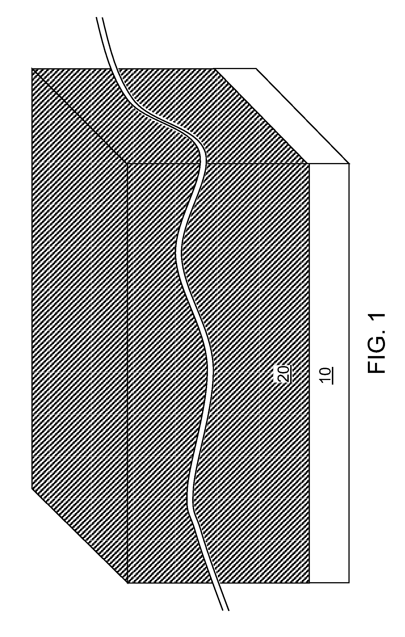
[0033]Referring to FIG. 1, a first exemplary structure according to the present disclosure includes a substrate, which includes a silicon layer 20 having a first conductivity type and a first conductive material layer 10. The substrate can consist of a stack of the first conductive material layer 10 and the silicon layer 20, or can further include at least another layer located at the bottom of the first conductive material layer 10 such as a dielectric substrate (such as a glass substrate or any other dielectric substrate) or another conductive material layer. For example, the first conductive material layer 10 can be a metallic layer including a metallic material. The metallic material can be aluminum, copper, or any other elemental metal or a conductive metallic alloy. The first conductive material layer 10 is a first conductive plate that functions as a first electrode of a photovoltaic device to be formed.

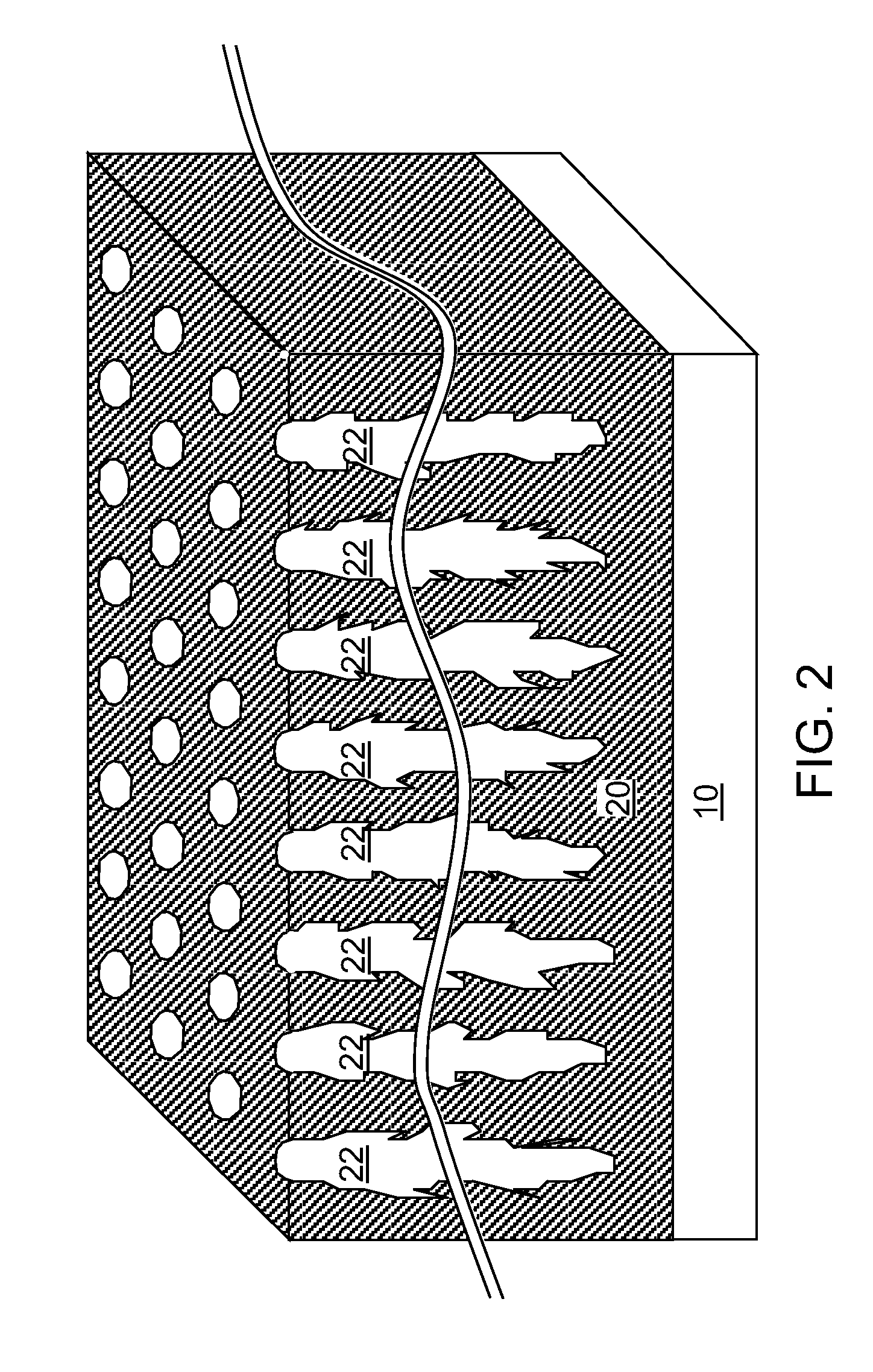
[0034]The silicon layer 20 includes silicon and at least one dopant havin...

second embodiment

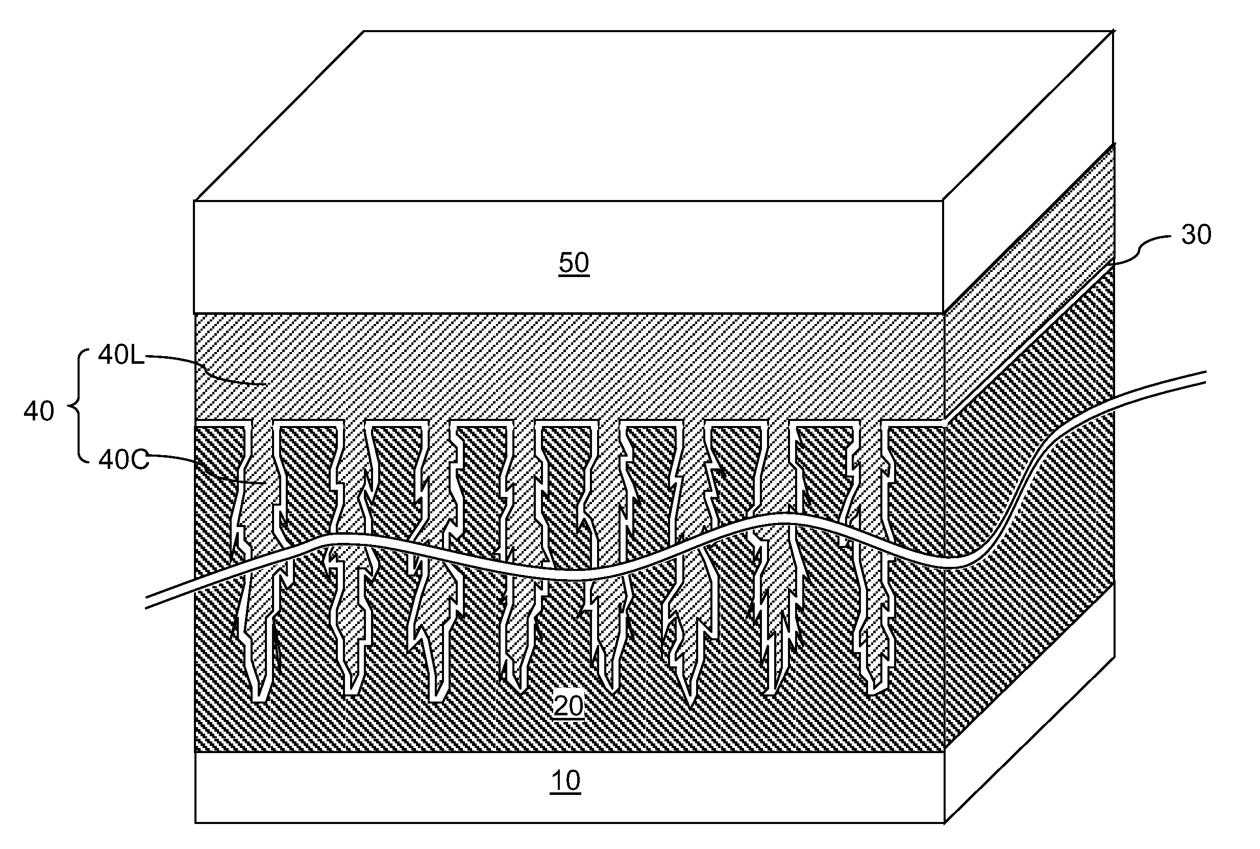
[0061]Referring to FIG. 8, a second exemplary structure according to the present disclosure is derived from the first exemplary structure of FIGS. 2 and 2 A by depositing an intrinsic semiconductor material layer 30 directly on surfaces of the array of nanopores 22 and the planar top surface 20T of the silicon layer 20. The intrinsic semiconductor material layer 30 includes an intrinsic semiconductor material.

[0062]The intrinsic semiconductor material in the intrinsic semiconductor material layer can include silicon, germanium, a silicon-containing alloy that may contain carbon or germanium, a germanium-containing alloy that may contain carbon or silicon, and / or a compound semiconductor material. The intrinsic semiconductor material can be a hydrogenated semiconductor material in which the hydrogen atoms reduce the dangling bonds of semiconductor atoms therein.

[0063]The intrinsic semiconductor material layer 30 can be deposited by an electrodeposition process employing a non-aqueous...


PUM


Abstract

A low-cost method is provided for forming a photovoltaic device, which is a high-performance nanostructured multijunction cell. The multiple P-N junctions or P-I-N junctions are contiguously joined to form a single contiguous P-N junction or a single contiguous P-I-N junction. The photovoltaic device integrates vertically-aligned semiconductor nanowires including a doped semiconductor material with a thin silicon layer having an opposite type of doping. This novel hybrid cell can provide a higher efficiency than conventional photovoltaic devices through the combination of the enhanced photon absorptance, reduced contact resistance, and short carrier transport paths in the nanowires. Room temperature processes or low temperature processes such as plasma-enhanced chemical vapor deposition (PECVD) and electrochemical processes can be employed for fabrication of this photovoltaic device in a low-cost, scalable, and energy-efficient manner.

Description

CROSS REFERENCE TO RELATED APPLICATION[0001]This application claims benefit from U.S. Provisional application Ser. No. 12 / 907,476, filed Oct. 19, 2010 the entire content and disclosure of which is incorporated herein by reference.STATEMENT REGARDING FEDERALLY SPONSORED RESEARCH OR DEVELOPMENT[0002]This invention was made with government support under Contract No. DE-AC05-00OR22725 awarded by the U.S. Department of Energy. The government has certain rights in this invention.FIELD OF THE INVENTION[0003]The present invention relates to a photovoltaic device, and particularly to a photovoltaic device including semiconductor nanowires, and methods of manufacturing the same.BACKGROUND OF THE INVENTION[0004]The majority of solar photovoltaic modules are silicon-based. Conventional solar cells are single junction devices in which the junction extends over a large planar region and formed in a high qualify single crystalline silicon substrate. Fabrication of such solar cells requires high pr...

Claims


Application Information

Patent Timeline
Patent Type & Authority Applications(United States)
IPC IPC(8): H01L31/0352B82Y40/00B82Y99/00
CPCH01L31/0284H01L31/035227B82Y30/00Y02E10/547H01L31/1804Y02P70/50
Inventor QU, JUNBESMANN, THEODORE M.DAI, SHENGZHANG, XIAOGUANG
Owner UT BATTELLE LLC
Why Eureka
Try Eureka