Magnetron sputtering apparatus and method

a sputtering apparatus and sputtering technology, applied in the direction of electrolysis components, vacuum evaporation coatings, coatings, etc., can solve the problems of difficult uniform formation of erosion b, low deposition efficiency as about 10%, and inability to obtain high deposition rate, so as to improve the deposition efficiency and the utilization efficiency of a target, the effect of low resistance film

Inactive Publication Date: 2013-04-04
TOKYO ELECTRON LTD
View PDF13 Cites 10 Cited by
  • Summary
  • Abstract
  • Description
  • Claims
  • Application Information

AI Technical Summary

Benefits of technology

[0025]In view of the above, the present invention provides a technique capable of improving the deposition efficiency and the utilization efficiency of a target while ensuring the in-plane uniformity of the deposition rate. The present invention also provides a technique capable of forming a low resistance film at a high deposition rate.

Problems solved by technology

However, in the above-described array of magnets, it is difficult to uniformly form the erosion 17 in the radial direction of the target 13.
However, in this configuration, since the amount of sputtered particles adhering to the anti-adhesion shield becomes larger as described above, the deposition efficiency is very low as about 10% and a high deposition rate cannot be obtained.
Thus, in the conventional magnetron sputtering apparatus, it is difficult to make the uniformity of the deposition rate compatible with the deposition efficiency.
In the above configuration, it is possible to ensure the deposition rate by increasing the applied power to, e.g., about 15 kWh; however, the mechanism is complex, the operation rate is low, and the manufacturing cost becomes high.
However, in the outer periphery of the magnet array, since there exists an open end where a vector direction of E×B is toward the outside of the target by the arrangement of N and S, electrons jump out of the outer periphery of the target, and electron loss becomes large.
In this case, since the open end is located near the outer periphery of the target, if electrons jump out of the outer periphery of the target, sparse and dense of the electron density may occur in the circumferential direction at the outer periphery, or the electron density may decrease in the radial direction of the target, which results in the non-uniformity of the electron density.
Further, since the magnetic flux near the open end diverges, the flux balance is lost, and the non-uniformity of the electron density increases.
In the array of only the point-shaped magnets, although the horizontal magnetic field generated between the magnets expands two-dimensionally by the magnet array, sufficient plasma density cannot be obtained, and it is difficult to ensure the in-plane uniformity of high plasma density.
Consequently, the utilization efficiency of the target is reduced.
However, if there is a strong magnetic field between the target and the shield member, it may cause abnormal discharge.
However, the above-cited references have not been focused on narrowing the distance between the target and the substrate and improving the efficiency of deposition while ensuring the in-plane uniformity of the deposition rate.
However, in the conventional technology, in addition to the problem that the deposition efficiency and the utilization efficiency of the target are low as described above, there is a problem such that there is a trade-off relationship between forming the tungsten (W) film to have a low resistance and obtaining a high deposition rate.
It is difficult to apply this technique to a general sputtering technology.
Further, although it can be recrystallized to have a low resistance by annealing after deposition, since a higher temperature of 1000° C. is necessary, it is not allowed in the semiconductor manufacturing process.
However, in combination of W and Ar, under low pressure, Ar ions make an elastic collision with the W film that is the target to be converted into neutral Ar atoms which rebound, and rush into the W film deposited on the substrate to cause damage.
It is obvious that it could be a cause generating a large amount of defects in the film.
Also, the amount of Ar in the film increases, which becomes a cause of the increase in resistance along with the defects.
Accordingly, the defects of the film further increase, and the resistivity of the film increases.
Since Kr is larger than Ar in both the mass and volume, the energy there of when rebounding is relatively small, and it is considered that it is difficult for Kr to get into the W film.
However, since Kr gas is at least 100 times more expensive than Ar gas, it is difficult to use the Kr gas in the semiconductor manufacturing process.
As a result, there is formed a film having many defects and an orientation that is not aligned.
However, in the conventional magnetron sputtering apparatus, since the distance between the target and the substrate is long and a discharge is caused under low pressure, the density of the plasma in the vicinity of the substrate is low and it is necessary to convert the Ar ions into high-energy ions.
Consequently, as described above, the Ar ions rush into the deposited W film to cause damage to the film.
This problem also occurs in the sputter deposition of other types of high melting point metal such as tantalum (Ta), titanium (Ti), molybdenum (Mo), ruthenium (Ru), hafnium (Hf), cobalt (Co) and nickel (Ni).

Method used


Image

  • Magnetron sputtering apparatus and method
  • Magnetron sputtering apparatus and method
  • Magnetron sputtering apparatus and method

Examples


example 1

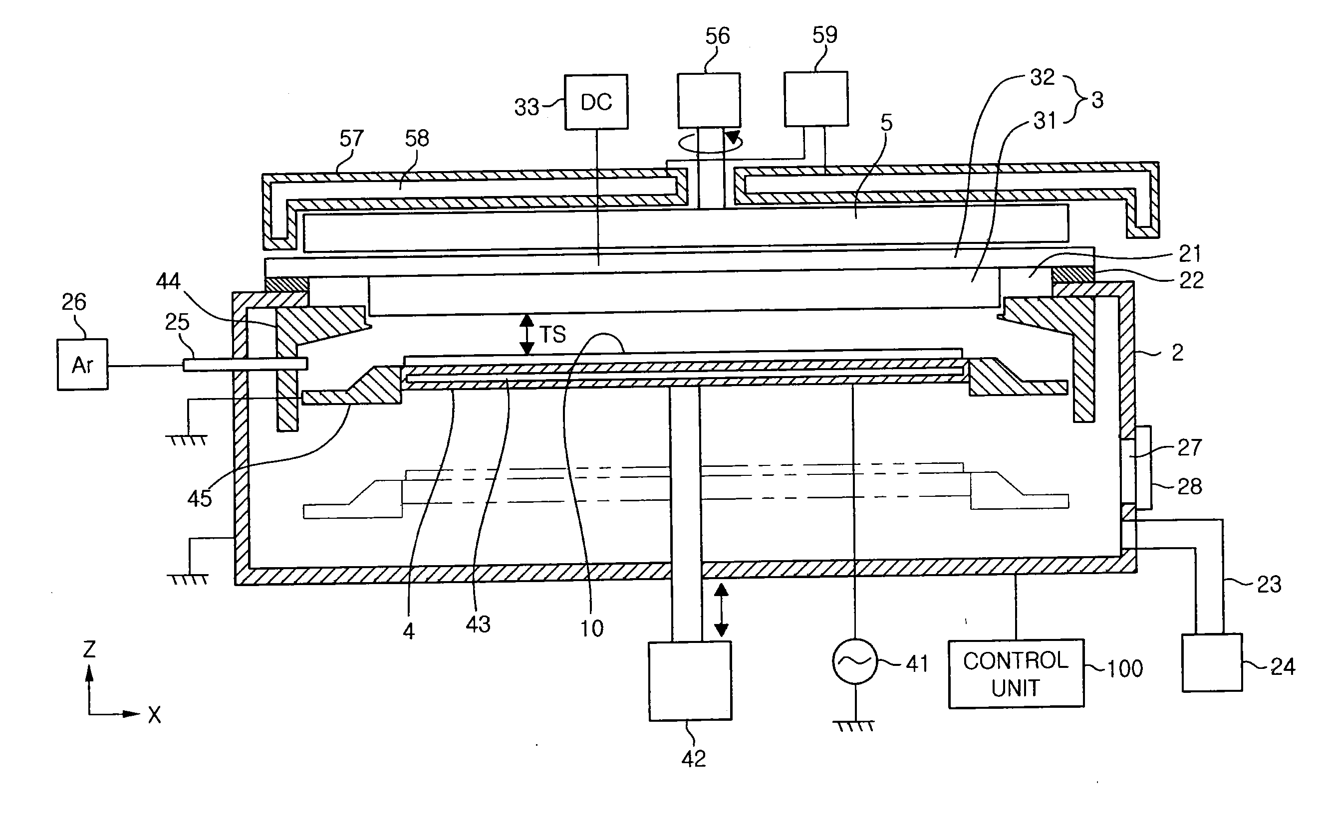
[0177]In the magnetron sputtering apparatus including the magnet array body 511 of FIG. 11, a deposition process was carried out under the processing conditions described above, and the evaluation of the relationship between the current density and the DC voltage applied to the target electrode 3 was conducted. At this time, the distance between the target 31 and the wafer 10 was set to 30 mm. Further, a configuration (Comparative Example 1) in which the return magnets 531 are not provided in the magnet array body 511, a configuration (Comparative Example 2) using the conventional magnetron sputtering apparatus shown in FIG. 23, and a configuration (Comparative Example 3) in which the discharge is performed by applying a DC voltage without using magnets were also evaluated in the same manner.

[0178]FIG. 16 shows the results. In FIG. 16, the horizontal axis represents the DC voltage applied to the target electrode 3, and the vertical axis represents the current density between the waf...

example 2

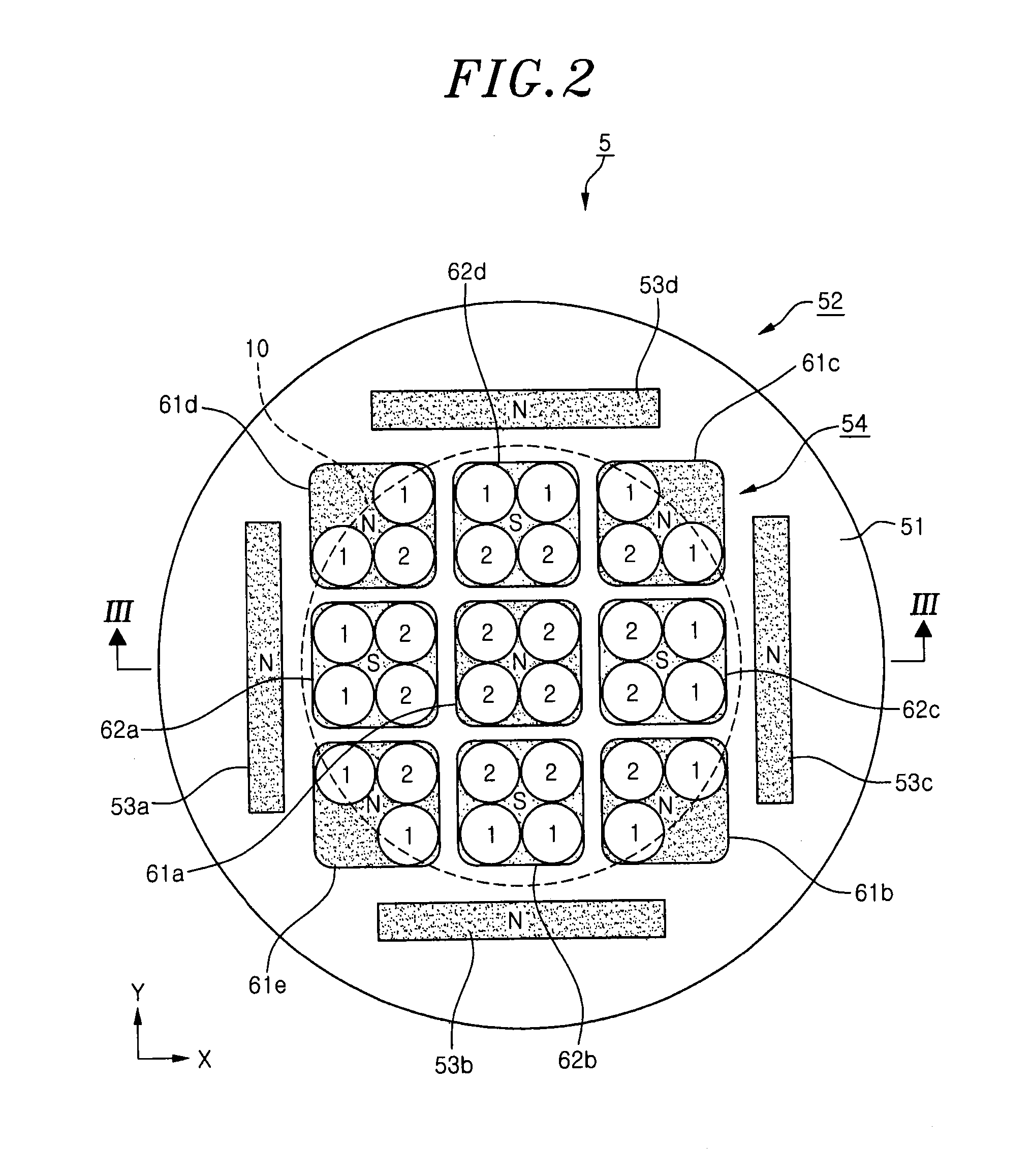
[0180]In the magnetron sputtering apparatus including the magnet array body 5 of FIG. 2, a deposition process was carried out under the processing conditions described above without rotating the magnet array body 5, and the deposition rate distribution in the radial direction of the wafer was obtained. Also in the case where the magnet array body 5A of FIG. 10 is provided instead of the magnet array body 5 of FIG. 2, the deposition rate was measured in the same manner. The results for the configuration in which the magnet array body 5 is provided are shown in FIG. 17, and the results for the configuration in which the magnet array body 5A is provided are shown in FIG. 18.

[0181]Here, a difference between the magnet array body 5 and the magnet array body 5A is only the number of the magnet elements 63 constituting the magnets 61 and 62. However, by adjusting the number of the magnet elements 63, it was observed that the deposition rate distribution in the radial direction of the wafer...

example 3

[0184]In the magnetron sputtering apparatus including the magnet array body 5 of FIG. 2, the distance between the target 31 and the wafer 10 was set to 20 mm, and a deposition process was carried out under the processing conditions described above without rotating the magnet array body 5 to obtain the deposition rate distribution in the radial direction of the wafer. Also in the case where the distance between the target 31 and the wafer 10 was set to 50 mm, the deposition rate was measured in the same manner. The results are shown in FIG. 19 along with the array of the magnet group 52 of the magnet array body 5 and the state of the erosion of the target 31. Further, in Example 3, the target 31 larger than the magnet group 52 of the magnet array body 5 was used.

[0185]Thus, it was observed that when the distance between the target 31 and the wafer 10 is 20 mm, the in-plane uniformity of the deposition rate is higher than that when the distance is 50 mm. Further, it was confirmed that...


PUM

PropertyMeasurementUnit
distanceaaaaaaaaaa
diameteraaaaaaaaaa
diameteraaaaaaaaaa

Abstract

A magnetron sputtering apparatus in which a target is disposed to face a substrate includes a magnet array body including a magnet group arranged on a base body, and a rotating mechanism for rotating the magnet array body around an axis perpendicular to the substrate. In the magnet array body, N poles and S poles constituting the magnet group are arranged to be spaced from each other along a surface facing the target such that a plasma is generated based on a drift of electrons by a cusp magnetic field. Magnets located on the outermost periphery of the magnet group are arranged in a line to prevent the electrons from being released from constraint of the cusp magnetic field and jumping out of the cusp magnetic field. A distance between the target and the substrate during sputtering is equal to or less than 30 mm.

Description

CROSS-REFERENCE TO RELATED APPLICATION[0001]This application claims priority to Japanese Patent Application Nos. 2011-216104 and 2012-172387 filed on Sep. 30, 2011 and Aug. 2, 2012, respectively, the entire contents of which are incorporated herein by reference.FIELD OF THE INVENTION[0002]The present invention relates to a magnetron sputtering apparatus and method.BACKGROUND OF THE INVENTION[0003]A magnetron sputtering apparatus used in a manufacturing process of semiconductor devices, for example, as shown in FIG. 33, is configured such that a target 13 made of a film forming material is disposed to face a substrate 12 in a vacuum chamber 11 set to a low pressure atmosphere, a magnet body 14 is provided at the top side of the target 13, and if the target 13 is a conductor such as metal, a magnetic field is formed in the vicinity of the lower surface of the target 13 in a state where a negative DC voltage is applied. Further, there is provided an anti-adhesion shield (not shown) to ...

Claims


Application Information

Patent Timeline
Patent Type & Authority Applications(United States)
IPC IPC(8): C23C14/35
CPCC23C14/35H01J37/32688H01J37/3455H01J37/3452H01J37/3405H01L21/203
Inventor MIZUNO, SHIGERUTOSHIMA, HIROYUKIGOMI, ATSUSHIMIYASHITA, TETSUYAHATANO, TATSUOMIZUSAWA, YASUSHI
Owner TOKYO ELECTRON LTD
Why Eureka
Try Eureka