Assist layers for EUV lithography

a technology of euv lithography and support layers, which is applied in the direction of photosensitive materials, instruments, photomechanical equipment, etc., can solve the problems of lack of powerful radiation sources, low throughput, and hinder the use of euv lithography, so as to improve resist performance, enhance photoresist's acid generation efficiency, and improve lwr and sensitivity

Active Publication Date: 2013-05-23
BREWER SCI
View PDF2 Cites 25 Cited by
  • Summary
  • Abstract
  • Description
  • Claims
  • Application Information

AI Technical Summary

Benefits of technology

[0037]The photoresist layer can be formed by any conventional method, with one preferred method being spin coating the photoresist composition at speeds of from about 350 rpm to about 4,000 rpm (preferably from about 1,000 rpm to about 2,500 rpm) for a time period of from about 20 seconds to about 90 seconds (preferably from about 30 seconds to about 60 seconds). The photoresist layer is then preferably post-application baked (“PAB”) at a temperature of at least about 90° C., preferably from about 100° C. to about 140° C., and more preferably from about 105° C. to about 130° C., and for time periods of from about 30 seconds to about 120 seconds. The thickness of the photoresist layer after baking will typically be from about 40 nm to about 120 nm, preferably from about 45 nm to about 80 nm, and more preferably from about 50 nm to about 70 nm.
[0038]The photoresist layer is subsequently patterned by exposure to EUV radiation for a dose of from about 1 mJ/cm2 to about 100 mJ/cm2, preferably from about 5 mJ/cm2 to about 50 mJ/cm2, and more preferably from about 5 mJ/cm2 to about 15 mJ/cm2, followed by development of the exposed photoresist layer. More specifically, the photoresist layer is exposed using a mask positioned above the surface of the photoresist layer. The mask has open areas designed to permit the EUV radiation to reflect from the mask and contact the surface of the photoresist layer. The remaining portions of the mask are designed to absorb the light to prevent the radiation from contacting the surface of the photoresist layer in certain areas. Those skilled in the art will readily understand that the arrangement of open areas and absorbing portions is designed based upon the desired pattern to be formed in the photoresist layer and ultimately in the substrate.
[0039]It will be appreciated that the present invention differs from the prior art in that it does not rely on the resist or EUV source to improve resist performance. This concept is different from prior concepts that rely on changing the resist to achieve better LWR and sensitivity. Advantageously, as the photoresist layer is exposed to EUV radiation, the assist layer absorbance is modulated as a source of secondary electron generation. Because the resist and assist layer behave as a single layer in the inventive method, there are no reflection effects, and both materials absorb approximately the same amount of energy. The high-energy EUV photon, which has about 14 times the energy of that of the 193-nm wavelength, and the secondary electron generation enhance the photoresist's acid-generation efficiency, and therefore improve LWR and sensitivity. More advantageously, the assist layer can be designed with a specific chromophore to absorb a specific wavelength that will control the reflectivity of the out-of-band radiation, which will mitigate the negative effect of the out-of-band radiation
[0040]After EUV

Problems solved by technology

Unfortunately, EUV lithography has been hindered by a number of problems, one of the most notable being a lack of powerful radiation sources.
Because of the limited amount of energy available, lithography performance can suffer, and long exposure times are needed, resulting in low throughput.
The main challenge in material design, particularly with resists, is to simultaneously achieve the improvement in line width roughness (LWR) and sensit

Method used


Image

  • Assist layers for EUV lithography
  • Assist layers for EUV lithography
  • Assist layers for EUV lithography

Examples


example 1

Preparation of Coating Using Sol-Gel Silicon Platform

[0064]In this procedure, 7.498 grams of tetraethoxysilane (Gelest, Morrisville, Pa.), 4.998 grams of 2-(3,4-epoxycyclohexyl)ethyl trimethoxysilane (Gelest), 12.496 grams of methyltrimethoxysilane (Gelest), and 58.315 grams of PGME (Ultra Pure Solutions, Inc., Castroville, Calif.) were added to a round-bottom flask. Over a 10-minute period, a solution of 2.937 grams of acetic acid (Sigma Aldrich) and 13.756 grams of water was added to the flask while stirring. The round-bottom flask was Fitted with a distillation head, distillation column, and collection flask. The solution was heated at 95° C. for 5 hours. By-products (water and methanol) were removed during the reaction. The final solution was used as ML-2 (discussed below) directly, without further purification.

[0065]Next, 3.096 grams of ML-2, 0.155 grams of 1 wt % benzyltriethylammonium chloride (“BTEAC,” Alfa Aesar, Ward Hill, Mass.) in PGME, 67.724 grams of PGME, 29.025 grams...

example 2

Preparation of Coating Using Sol-Gel Silicon Platform

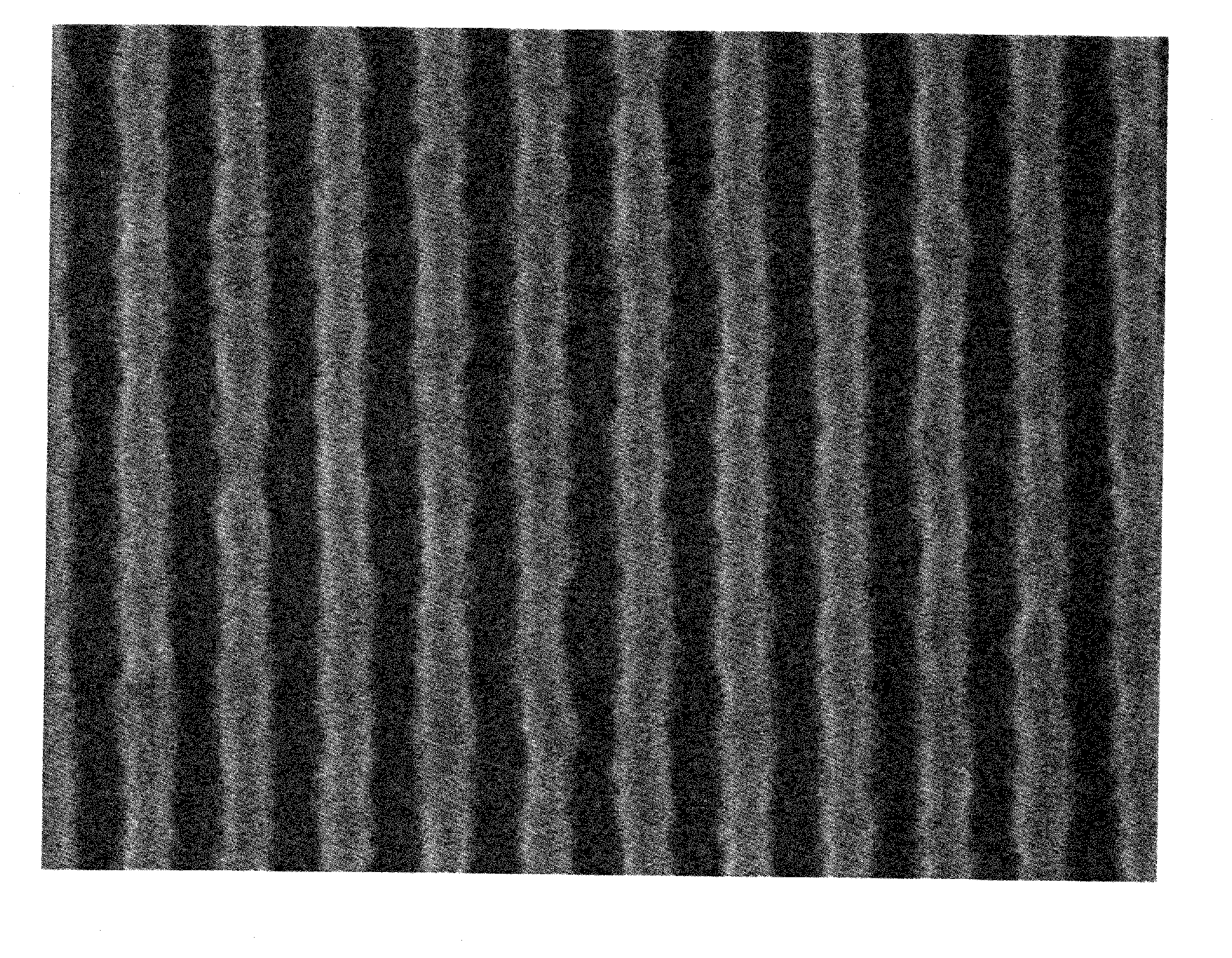
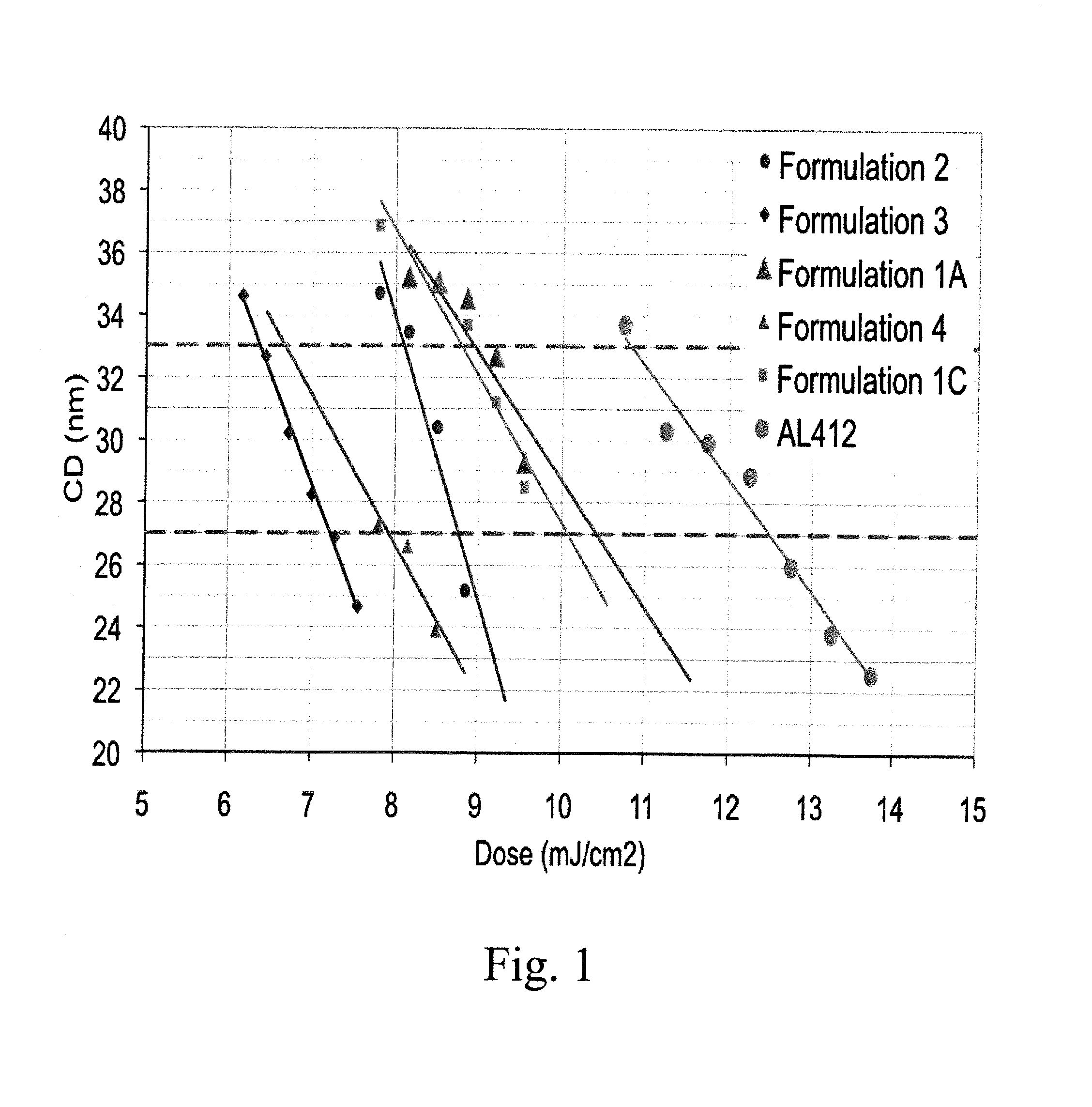
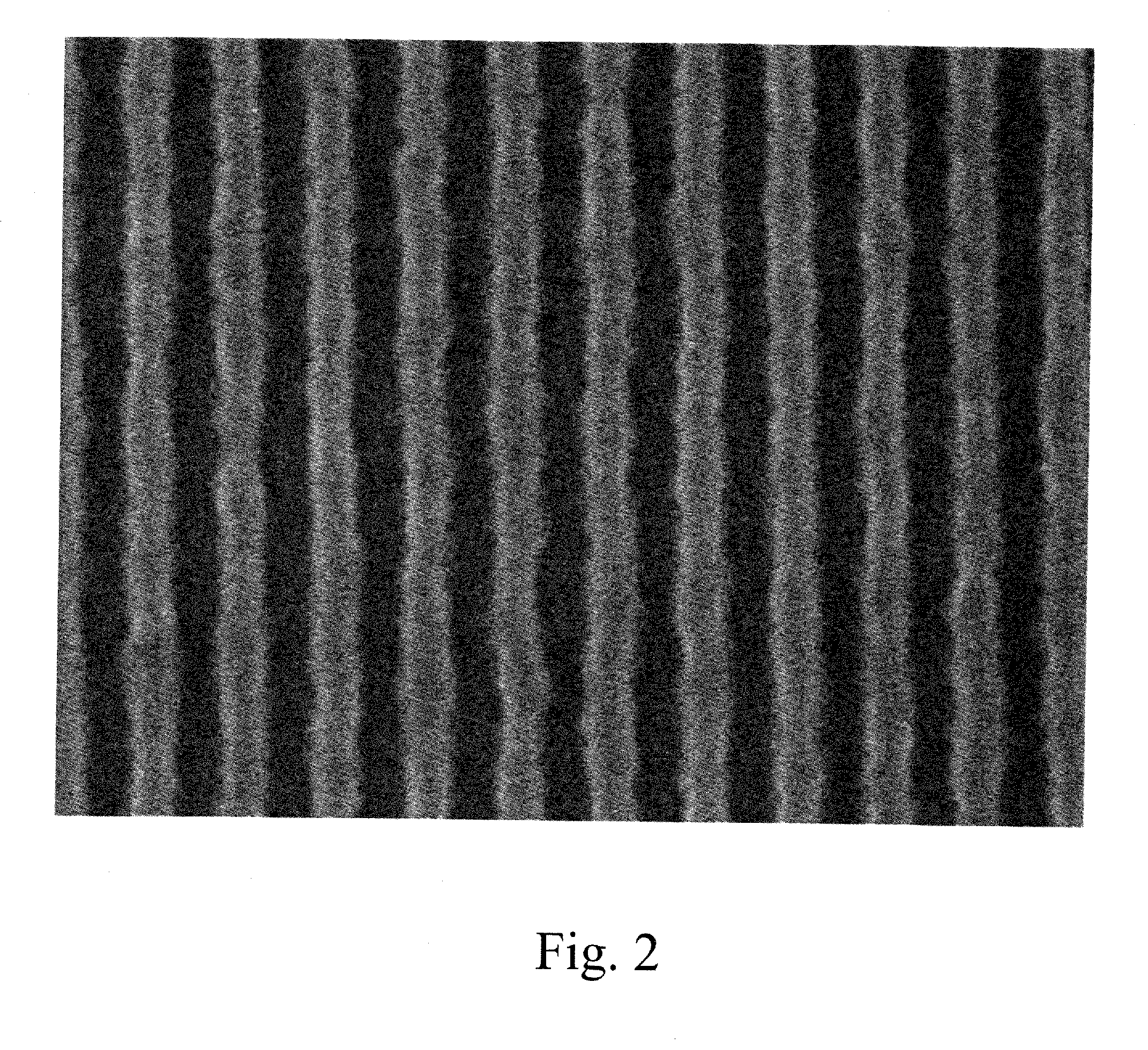
[0069]In this Example, 20.32 grams of tetraethoxysilane, 34.04 grams of 75% titanium diisopropoxide bis(−2,4-pentandionate) in isopropanol (Gelest), and 41.43 grams of PGME were added to a round-bottom flask. Over a 10-minute period, a solution of 0.70 gram of acetic acid (Sigma Aldrich) and 3.51 grams of water was added to the flask while stirring. The round-bottom flask was fitted with a distillation head, distillation column, and collection flask. The solution was heated at 95° C. for 5 hours. By-products (water and methanol) were removed during the reaction, after which 21.44 grams of the resulting solution, 5.52 grams of 0.55 wt % BTEAC in PGME, 25.10 grams of PGME, and 47.94 grams of PGMEA were mixed until homogeneous. The homogenous mixture was filtered through a 0.2-μm end-point filter to produce Formulation 2. Formulation 2 was formed into a 20-nm thick film by spin coating on a 4-inch silicon wafer at 1,500 rpm for 60 se...

example 3

Preparation of Coating Using Sol-Gel Silicon Platform

[0070]In this procedure, 15.23 grams of tetraethoxysilane, 34.20 grams of 60% zirconium di-n-butoxide bis(-2,4-pentandionate) in n-butanol (Gelest) and 46.25 grams of PGME (Ultra Pure Solutions, Inc.) were added to a round-bottom flask. Over a 10-minute period, a solution of 0.63 gram of acetic acid (Sigma Aldrich) and 2.69 grams of water was added to the flask while stirring. The round-bottom flask was fitted with a distillation head, distillation column, and collection flask. The solution was heated at 95° C. for 5 hours. By-products (water and methanol) were removed during the reaction, after which 21.86 grams of the resulting solution, 5.44 grams of 0.55 wt % BTEAC in PGME, 24.66 grams of PGME, and 48.04 grams of PGMEA were mixed until homogeneous. The homogeneous mixture was then filtered through a 0.2-μm end-point filter to produce Formulation 3. Formulation 3 was formed into a 20-nm thick film by spin coating on a 4-inch si...


PUM

PropertyMeasurementUnit
Percent by massaaaaaaaaaa
Nanoscale particle sizeaaaaaaaaaa

Abstract

The present invention provides novel methods of fabricating microelectronics structures, and the resulting structures formed thereby, using EUV lithographic processes. The method involves utilizing an assist layer immediately below the photoresist layer. The assist layer can either be directly applied to the substrate, or it can be applied to any intermediate layer(s) that may be applied to the substrate. The preferred assist layers are formed from spin-coatable, polymeric compositions. The inventive method allows reduced critical dimensions to be achieved with improved dose-to-size ratios, while improving adhesion and reducing or eliminating pattern collapse issues.

Description

RELATED APPLICATIONS[0001]The present application claims the priority benefit of U.S. Provisional Patent Application Ser. No. 61 / 562,166, filed Nov. 21, 2011, entitled ASSIST LAYERS FOR EUV LITHOGRAPHY, incorporated by reference in its entirety herein.BACKGROUND OF THE INVENTION[0002]1. Field of the Invention[0003]This invention is concerned with methods of fabricating microelectronic structures using EUV (extreme ultraviolet) lithography.[0004]2. Description of the Prior Art[0005]As the semiconductor industry continues to follow Moore's law, the demand for ever-decreasing feature sizes requires the use of thinner films to prevent pattern collapse. Thinner films will require using a hardmask to transfer the pattern to the substrate. Extreme ultraviolet (EUV) exposure is expected to be the method of choice for single exposure lithography to achieve the required critical dimension (CD) targets of the 22-nm node and beyond. Unfortunately, EUV lithography has been hindered by a number o...

Claims


Application Information

Patent Timeline
IPC IPC(8): G03F7/09G03F7/20
CPCB82Y30/00G03F7/092G03F7/2004Y10T428/24917G03F7/11B82Y40/00Y10S977/755H01L21/0273H01L21/0274
Inventor OUATTARA, TANTIBOROWASHBURN, CARLTON A.KRISHNAMURTHY, VANDANAGUERRERO, DOUGLAS
Owner BREWER SCI
Why Eureka
Try Eureka