Replacement Gate With Reduced Gate Leakage Current
- Summary
- Abstract
- Description
- Claims
- Application Information
AI Technical Summary
Benefits of technology
Problems solved by technology
Method used
Image
Examples
first embodiment
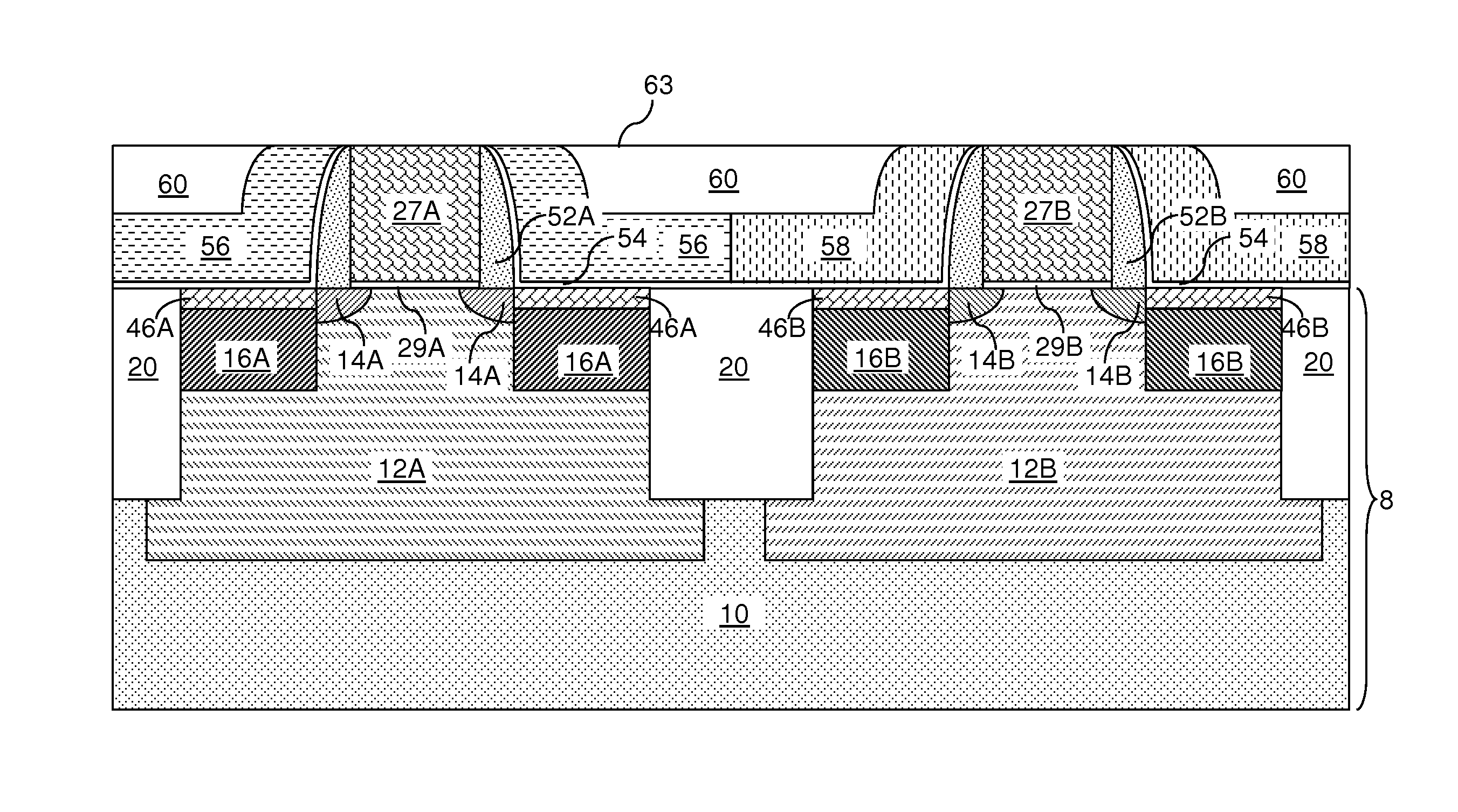
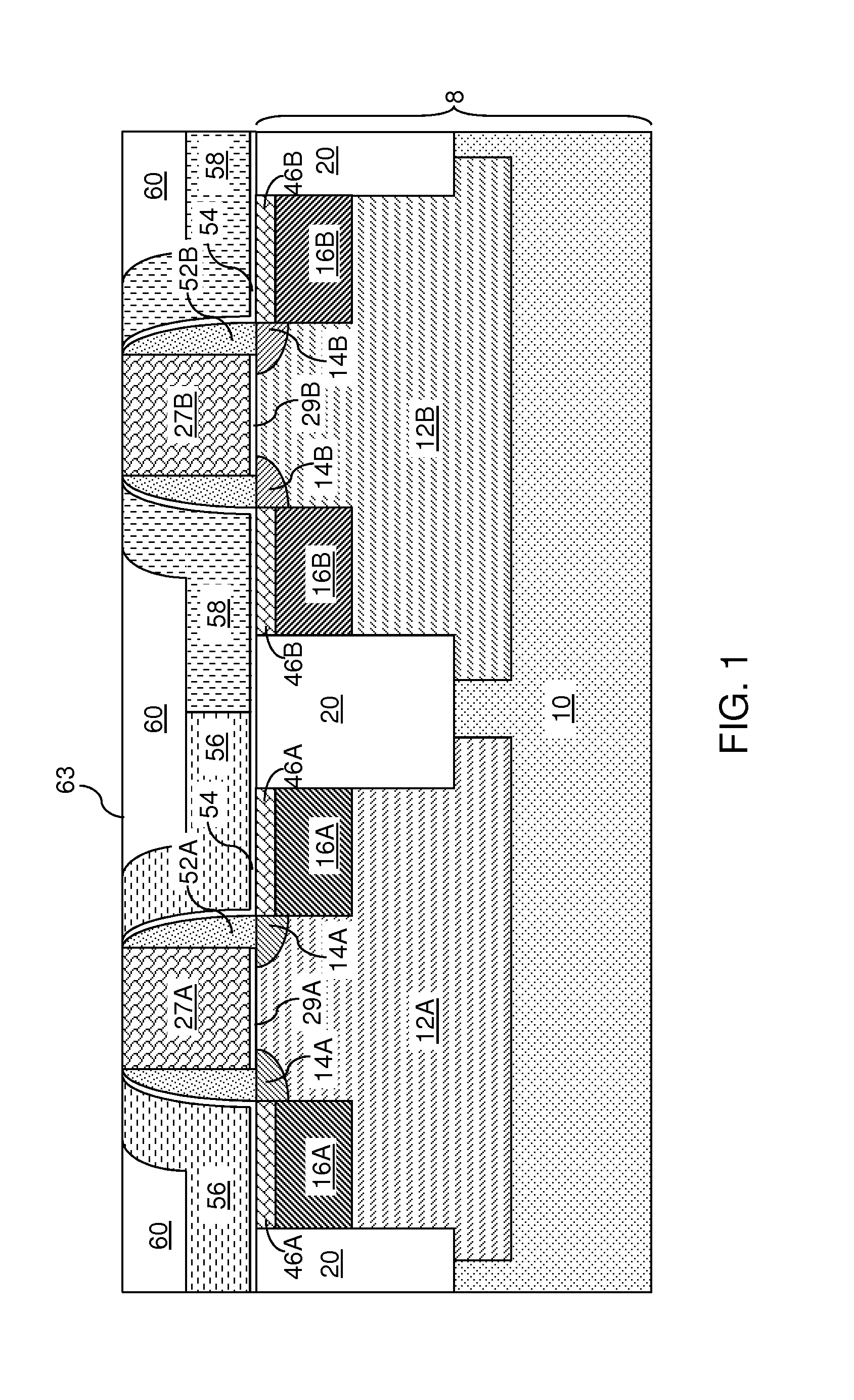
[0037]Referring to FIG. 1, a first exemplary semiconductor structure according to the present disclosure includes a semiconductor substrate 8, on which various components of field effect transistors are formed. The semiconductor substrate 8 can be a bulk substrate including a bulk semiconductor material throughout, or a semiconductor-on-insulator (SOI) substrate (not shown) containing a top semiconductor layer, a buried insulator layer located under the top semiconductor layer, and a bottom semiconductor layer located under the buried insulator layer.
[0038]Various portions of the semiconductor material in the semiconductor substrate 8 can be doped with electrical dopants of n-type or p-type at different dopant concentration levels. For example, the semiconductor substrate 8 may include an underlying semiconductor layer 10, a first doped well 12A formed in a first device region (the region to the left in FIG. 1), and an second doped well 12B formed in a second device region (the regi...
second embodiment
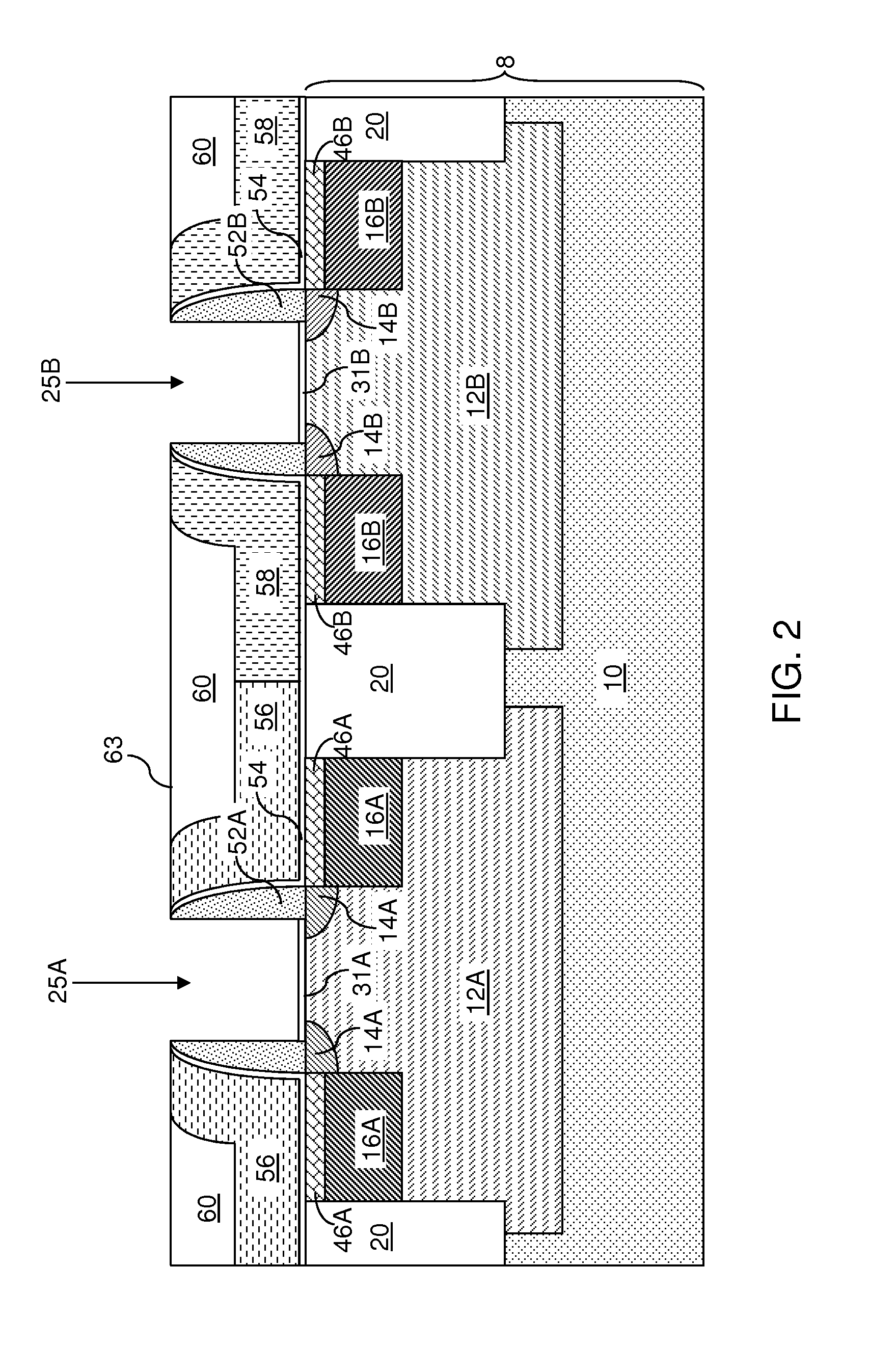
[0094]Referring to FIG. 19, a second exemplary semiconductor structure according to the present disclosure is derived from the first exemplary semiconductor structure of FIG. 1A by removing the first and second disposable gate material portions (27A, 27B) selective to the dielectric materials of the planarization dielectric layer 60, the first stress-generating liner 58 and / or the second stress-generating liner 56 (if present), and the first and second dielectric gate spacers (52A, 52B). The disposable dielectric portions (29A, 29B) may, or may not, be removed at this step.
[0095]An optional dielectric liner 230L may be applied over the planarization dielectric layer 60 and within the first and second gate cavities (25A, 25B; See FIG. 2). A photoresist layer 239 is applied over the optional dielectric liner 230L or over the planarization dielectric layer 60 and within the first and second gate cavities (25A, 25B). The photoresist layer 239 is lithographically patterned by lithographi...
third embodiment
[0099]Referring to FIG. 23, a third exemplary semiconductor structure according to the present disclosure is derived from the first exemplary semiconductor structure of FIG. 1A by removing the first and second disposable gate material portions (27A, 27B) selective to the dielectric materials of the planarization dielectric layer 60, the first stress-generating liner 58 and / or the second stress-generating liner 56 (if present), and the first and second dielectric gate spacers (52A, 52B). The disposable dielectric portions (29A, 29B) may, or may not, be removed at this step.
[0100]An optional dielectric liner 230L may be applied over the planarization dielectric layer 60 and within the first and second gate cavities (25A, 25B; See FIG. 2). A photoresist layer 239 is applied over the optional dielectric liner 230L or over the planarization dielectric layer 60 and within the first and second gate cavities (25A, 25B). The photoresist layer 239 is lithographically patterned by lithographic...
PUM
 Abstract
Description
Claims
Application Information


