
Al-sb-te phase change material used for phase change memory and fabrication method thereof

Active Publication Date: 2013-12-19
SHANGHAI INST OF MICROSYSTEM & INFORMATION TECH CHINESE ACAD OF SCI
View PDF10 Cites 3 Cited by
  • Summary
  • Abstract
  • Description
  • Claims
  • Application Information

AI Technical Summary

Benefits of technology

The present invention provides an Al—Sb—Te phase change material that can be used for PCM (phase change memory) with good thermal stability, fast crystallization speed, low power consumption and compatibility with CMOS process. The material has a high difference in resistance before and after phase change, making it an ideal PCM material. It can be adjusted to have different crystallization temperatures, melting temperatures, and activation energies of crystallization, and can be used for stable operation under high temperature conditions. The material has a small volume difference before and after phase change and good data retention.

Problems solved by technology

As a mainstream non-volatile memory, flash technology has encountered the bottleneck.
The technical weakness becomes more highlighted with the development of integrated circuits.
Limitations such as low speed, high write voltage and limited number of cycles have directly restricted further application of flash technology.
Ge2Sb2Te2 is a typical phase change material used for PCM, but it is found in actual applications that, due to great change of density and poor crystallization speed (about hundreds of ns generally) of Ge2Sb2Te2 material during phase change, the erase and write speed and the device reliability are influenced; furthermore, low crystallization temperature of about 160° C. makes it difficult to be used under high temperature conditions.

Method used


Image

  • Al-sb-te phase change material used for phase change memory and fabrication method thereof
  • Al-sb-te phase change material used for phase change memory and fabrication method thereof

Examples


embodiment 1

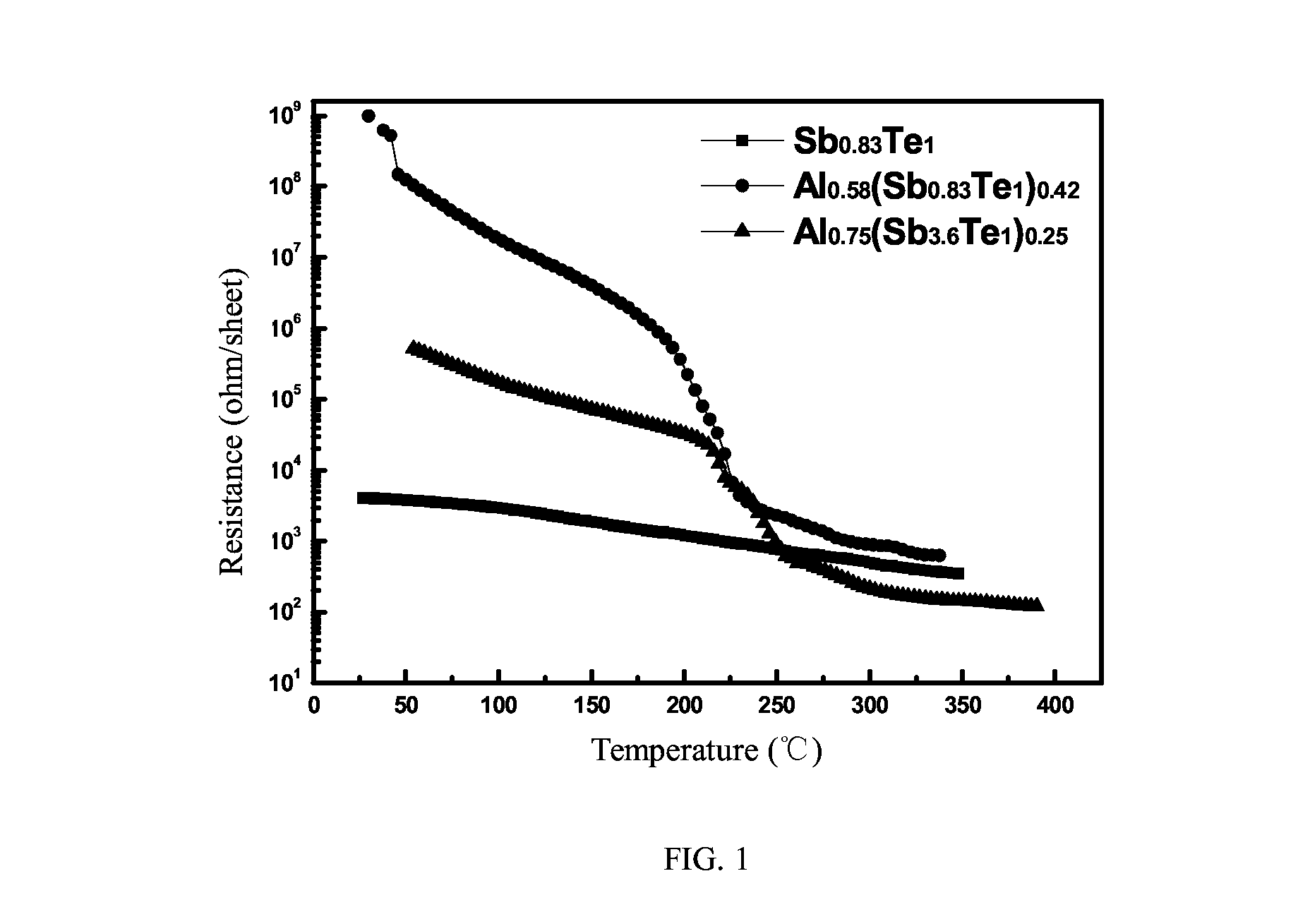
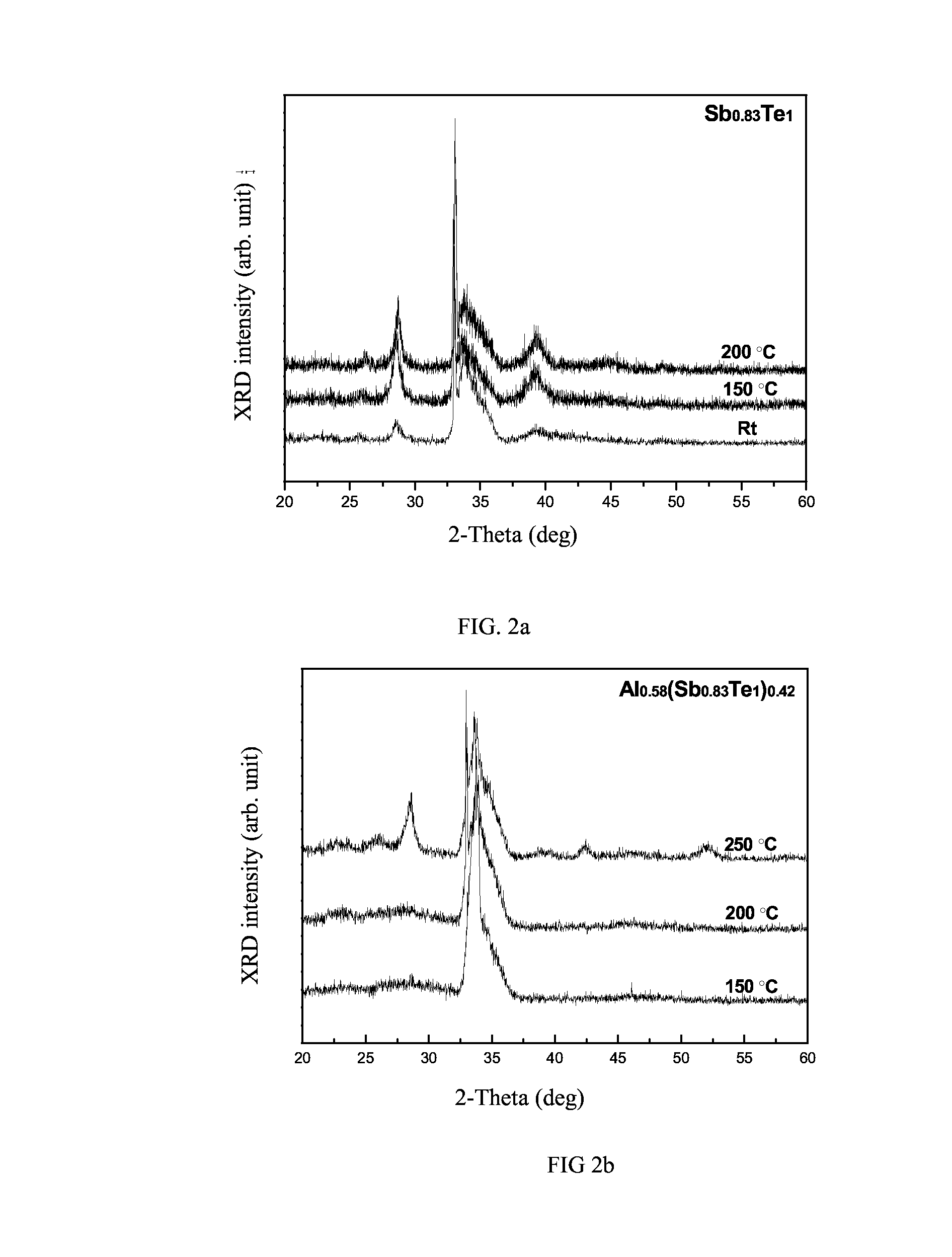
[0023]The technical scheme of the present invention is further detailed by the preparation of Alx(SbyTe1)1-x phase change material and the test thereof in this embodiment. Detailed preparation method is described as follow:[0024](1) Prepare Al—Sb—Te thin film on regular silicon substrate and thermally oxidized silicon substrate simultaneously by magnetron co-sputtering with two targets, wherein a base vacuum level is 1.8×10⁻⁴ Pa and a sputtering argon pressure is 0.21 Pa. Film materials with three compositions are prepared under the conditions mentioned above, wherein the parameters of each composition is shown in the table below:

Film growthRateArtime (min) Film(nm / Source power(sccm)thickness(nm)Compositionmin)Sb0.83Te1 -RF20w2030 / 120Sb0.83Te14Al-DC15w2030 / 150Al0.585Sb0.83Te1 -RF20w(Sb0.83Te1)0.42Al-DC15w2030 / 210Al0.757Sb0.83Te1 -RF20w(Sb3.6Te1)0.25Sb- RF20w[0025](2) The resistance of the as-deposited Alx(SbyTe1)1-x film grown on the oxidized silicon substrate is in situ measured, a...


PUM

PropertyMeasurementUnit
Timeaaaaaaaaaa
Timeaaaaaaaaaa
Thicknessaaaaaaaaaa

Abstract

The present invention discloses an Al—Sb—Te phase change material used for PCM and fabrication method thereof. Said phase change material, which can be prepared by PVD, CVD, ALD, PLD, EBE, and ED, is a mixture of three elements aluminum (Al), antimony (Sb) and tellurium (Te) with a general formula of Alx(SbyTe1)1-x, where 0<x≦0.85, 0.67≦y≦7. Said material is electrically driven from outside. By adjusting the content of three elements in the mixture, storage materials with different crystallization temperatures, melting temperatures and activation energies of crystallization can be achieved. Any two elements of aluminum, antimony and tellurium can be bonded to each other, so the adjustability is very high, maintaining the phase change properties in a wide range. Compared with conventional Ge2Sb2Te5, the materials achieved by properly adjusting the element ratio in Alx(SbyTe1)1-x have higher crystallization temperatures, better thermal stability and data retention, and lower melting temperatures, while at the same time inheriting the fast phase change capability from SbyTe1. Moreover, as a common element used in microelectronics, aluminum (Al) features mature technology and nice compatibility with CMOS.

Description

FIELD OF THE INVENTION[0001]This invention relates to a phase change thin film used in the microelectronics field and fabrication method thereof, and more particularly to a phase change thin film composed of a mixture of aluminum-antimony-tellurium and fabrication method thereof.BACKGROUND OF THE INVENTION[0002]Memory enjoys a significant position in the semiconductor market, 10% of which is occupied by dynamic random access memory (DRAM) and flash alone. With the gradual popularity of portable electronic devices, a growing market for non-volatile memory can be expected, coupled with increasingly high requirements of consumers for the capacity, speed and etc. of memory. As a mainstream non-volatile memory, flash technology has encountered the bottleneck. The technical weakness becomes more highlighted with the development of integrated circuits. Limitations such as low speed, high write voltage and limited number of cycles have directly restricted further application of flash techno...

Claims


Application Information

Patent Timeline
IPC IPC(8): G11C11/56C23C14/14C01B19/00
CPCG11C11/56C01B19/007C23C14/14C23C14/0623C23C14/35G11C13/0004H10N70/231H10N70/8828
Inventor PENG, CHENGWU, LIANGCAIRAO, FANGSONG, ZHITANGLIU, BOZHOU, XILINZHU, MIN
Owner SHANGHAI INST OF MICROSYSTEM & INFORMATION TECH CHINESE ACAD OF SCI
Learn More