

Oxide sintered body and sputtering target
a technology of sputtering target and sintered body, which is applied in the direction of diaphragms, metallic material coating processes, electrical equipment, etc., can solve problems such as abnormal discharge, and achieve the effects of low specific resistance, reduced raw material cost, and high relative density
- Summary
- Abstract
- Description
- Claims
- Application Information
AI Technical Summary
Benefits of technology
Problems solved by technology
Method used
Image


Examples
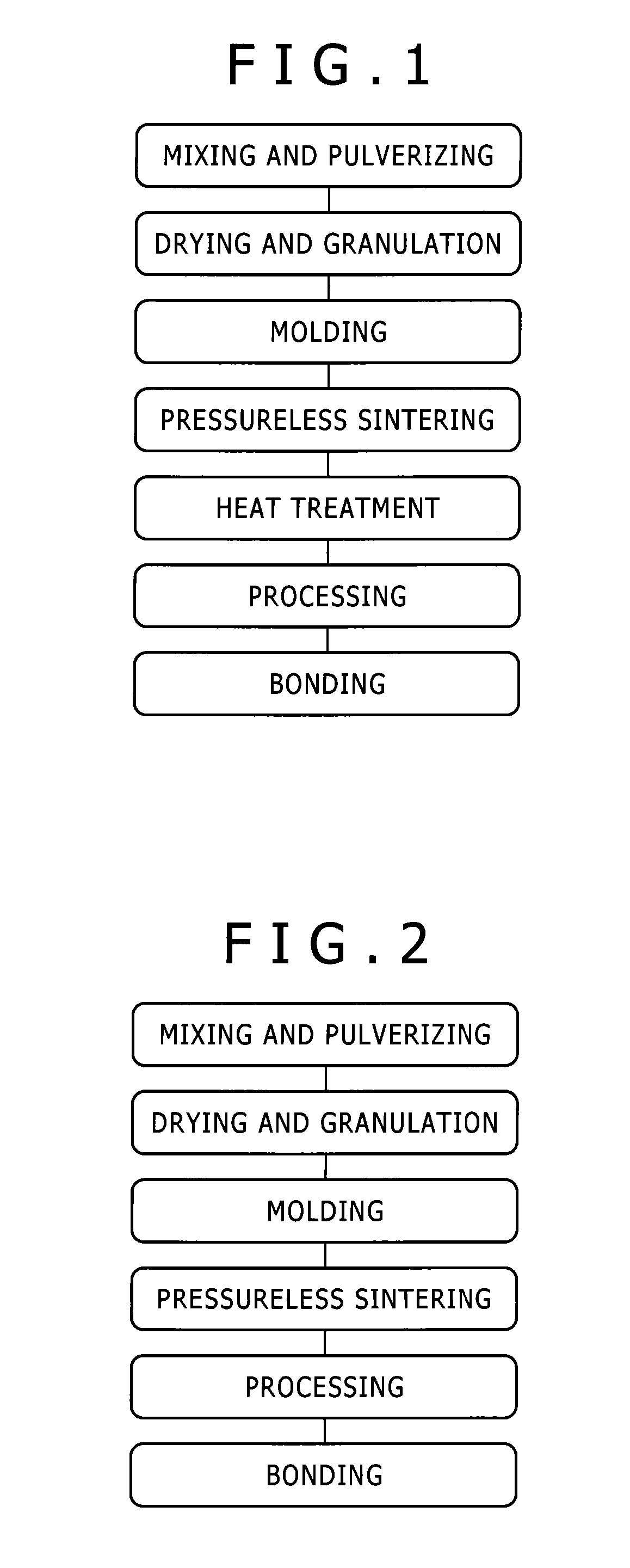
example 1
[0054]Zinc oxide powder (JIS1) having a purity of 99.99%, tin oxide powder having a purity of 99.99%, and aluminum oxide powder having a purity of 99.99% were blended at the ratio of [Zn] [Sn]:[Al]=73.9:24.6:1.5, and mixed by a nylon ball mill for 20 hours. For reference, Table 1 shows the Zn ratio and the Sn ratio. The Al ratio was 0.015. Then, the mixed powders obtained in the above process were dried and granulated, preformed at a molding pressure of 0.5 tonf / cm2 by the die press, and then mainly molded at a molding pressure of 3 tonf / cm2 by the CIP.
[0055]As shown in Table 1, the thus-obtained molded body was sintered while being held at 1500° C. under normal pressure for 7 hours. At this time, the sintering was performed under the oxygen atmosphere with oxygen gas introduced into a sintering furnace. Then, the sintered body was put in a heat treatment furnace, and subjected to heat treatment at 1200° C. for 10 hours. The heat treatment was performed under the reducing atmosphere...
example 2
[0060]Zinc oxide powder (JIS1) having a purity of 99.99%, tin oxide powder having a purity of 99.99%, and tantalum oxide powder having a purity of 99.99% were blended at the ratio of [Zn] [Sn]:[Ta]=73.9:24.6:1.5. The mixed powder was sintered at 1550° C. for 5 hours, and subjected to heat treatment at 1150° C. for 14 hours. Except for the above points, the same processes as those in Example 1 described above were performed in Example 2, which produced the oxide sintered body of Example 2 (Ta ratio=0.015).
[0061]The relative density and specific resistance of the thus-obtained oxide sintered body of Example 2 were measured in the same way as in the above Example 1. As a result, the relative density of the oxide sintered body was 90% or more, and the specific resistance thereof was 0.1 Ω·cm or less, so that good results were obtained.
[0062]Then, the above oxide sintered body was used to perform the DC (direct current) magnetron sputtering in the same way as in the above Example 1. As a...
example 3
[0065]Zinc oxide powder (JIS1) having a purity of 99.99%, tin oxide powder having a purity of 99.99%, and indium oxide powder having a purity of 99.99% were blended at the ratio of [Zn]:[Sn]:[In]=45.0:45.0:10.0. The mixed powder was sintered at 1550° C. for 5 hours (without the heat treatment). Except for the above points, the same processes as those in Example 1 described above were performed in Example 3, which produced the oxide sintered body of Example 3 (In ratio=0.10).
[0066]The relative density and specific resistance of the thus-obtained oxide sintered body of Example 3 were measured in the same way as in the above Example 1. As a result, the relative density of the oxide sintered body was 90% or more, and the specific resistance thereof was 0.1 Ω·cm or less, so that good results were obtained.
[0067]Then, the above oxide sintered body was used to perform the DC (direct current) magnetron sputtering in the same way as in the above Example 1. As a result, the occurrence of the ...
PUM
| Property | Measurement | Unit |
|---|---|---|
| distribution coefficient | aaaaa | aaaaa |
| specific resistance | aaaaa | aaaaa |
| relative density | aaaaa | aaaaa |
Abstract
Description
Claims
Application Information