Aluminium oxide-based metallisation barrier

a technology of aluminium oxide and a metallisation barrier, which is applied in the direction of liquid/solution decomposition chemical coating, semiconductor/solid-state device details, coatings, etc., can solve the problem of increasing the pressure of conventional full-area metallisation on the back, the surface recombination speed of the strongly aluminium-doped layer is very high, and cannot be further reduced as desired by means of existing conventional technology

Inactive Publication Date: 2013-12-26
MERCK PATENT GMBH
View PDF11 Cites 20 Cited by
  • Summary
  • Abstract
  • Description
  • Claims
  • Application Information

AI Technical Summary

Benefits of technology

[0024]The object is achieved, in particular, by a process for the production of a dielectric layer which acts as passivation layer and diffusion barrier against aluminium and / or other related metals and metal pastes, in which an aluminium oxide sol or an aluminium oxide hybrid sol in the form of an ink or paste is applied over the entire surface or in a structured manner and is compacted and dried by warming at elevated temperatures, forming amorphous Al2O3 and / or aluminium oxide hybrid layers. In this way, amorphous Al2O3 and / or aluminium oxide hybrid layers having a thickness of <100 nm are formed. In order to achieve a greater layer thickness of amorphous Al2O3 and / or aluminium oxide hybrid of at least 150 nm by this process, the aluminium oxide sol or aluminium oxide hybrid sol can be applied and dried a number of times in a particular embodiment of the process according to the invention. After application of the sol, the drying is carried out at temperatures between 300 and 1000° C., preferably in the range between 350 and 450° C. Good layer properties are achieved if this drying is carried out within a time of two to five minutes. Particularly good barrier-layer properties arise if the layer(s) applied and dried in accordance with the invention is (are) passivated by subsequent annealing at 400 to 500° C. in a nitrogen and / or forming-gas atmosphere.

Problems solved by technology

Ever-thinner solar wafers (current thickness 200-180 μm with a strong trend towards 160 μm) are causing ever more-pressing problems in conventional full-area metallisation on the back.
On the one hand, the surface recombination speed in the strongly aluminium-doped layer is very high (typically 500-1000 cm / s) and cannot be reduced further as desired by means of the existing conventional technology.
The consequence is a lower power output compared with more advanced, but also more expensive concepts, which is principally evident from lower short-circuit currents and reduced open terminal voltage.
This “bow” has an extremely disadvantageous effect during subsequent module assembly of the solar cells since a significantly increased breakage rate during manufacture is associated therewith.
These are predominantly technical production and technologically induced problems.
However, this technology also requires the production of the diffusion mask, the production of the local structuring of the diffusion mask and removal thereof, since this boron-interspersed diffusion mask itself cannot have a passivating action, and the creation of a layer which has a passivating action for the surface and, if necessary, encapsulation thereof.
Even this brief outline shows the difficulties which usually underlie this approach, besides technological problems of a general nature: time, industrial throughput and thus ultimately the costs of implementation.
The technology for the production of an LBSF solar cell by means of the LFC process is distinguished by high process costs for the deposition of the vapour-deposited aluminium layers, meaning that the possibility of industrial implementation of this concept has not yet been definitively answered.
However, not all above-mentioned materials and layer systems are suitable as diffusion-barrier layers of this type.
Silicon oxide is not resistant to penetration by aluminium paste.
This lack of resistance of the silicon oxide layer during firing is caused by the alumothermal process at high temperatures; to be precise, silicon oxide is less thermodynamically stable than aluminium oxide.
Silicon nitride, although suitable as passivation material, cannot, however, function as passivation material and diffusion-barrier layer since the problem of “parasitic shunting” is frequently observed at local contacts.
These layer stacks are applied to the wafer surface in a conventional manner by means of PVD and / or CVD methods and are thus system-inherently expensive and in some cases unsuitable for industrial production [cf., for example, coating with aluminium oxide by means of “atomic layer deposition” (ALD)].
A disadvantage in this process is that penetration points are not pre-specified for the metal paste.
A further disadvantage are the costs arising with the nitride coating.
This process is time-consuming and thus expensive, where the costs are influenced, inter alia, by the use of high-purity gases which are critical from occupational safety points of view (NH3 and SiH4).

Method used


Image

  • Aluminium oxide-based metallisation barrier
  • Aluminium oxide-based metallisation barrier
  • Aluminium oxide-based metallisation barrier

Examples


example 1

[0068]In accordance with Example 4 from the European patent application with the application number 11 001 920.5: 3 g of salicylic acid and 1 g of acetylacetone in 25 ml of isopropanol and 25 ml of diethylene glycol monoethyl ether are initially introduced in a 100 ml round-bottomed flask. 4.9 g of aluminium tri-sec-butoxide are added to the solution, and the mixture is stirred for a further 10 minutes. 5 g of acetic acid are added in order to neutralise the butoxide and adjust the pH of the ink, and the mixture is again stirred for 10 minutes. 1.7 g of water are added in order to hydrolyse the partially protected aluminium alkoxide, and the slightly yellow solution is stirred for 10 minutes and left to stand in order to age. The solids content can be increased to 6% by weight. The ink exhibits a stability of >3 months with ideal coating properties and efficient drying (cf. FIGS. 1 and 2 in the above-mentioned patent application 11 001 920.5).

[0069]In order to evaluate the metal-bar...

example 2

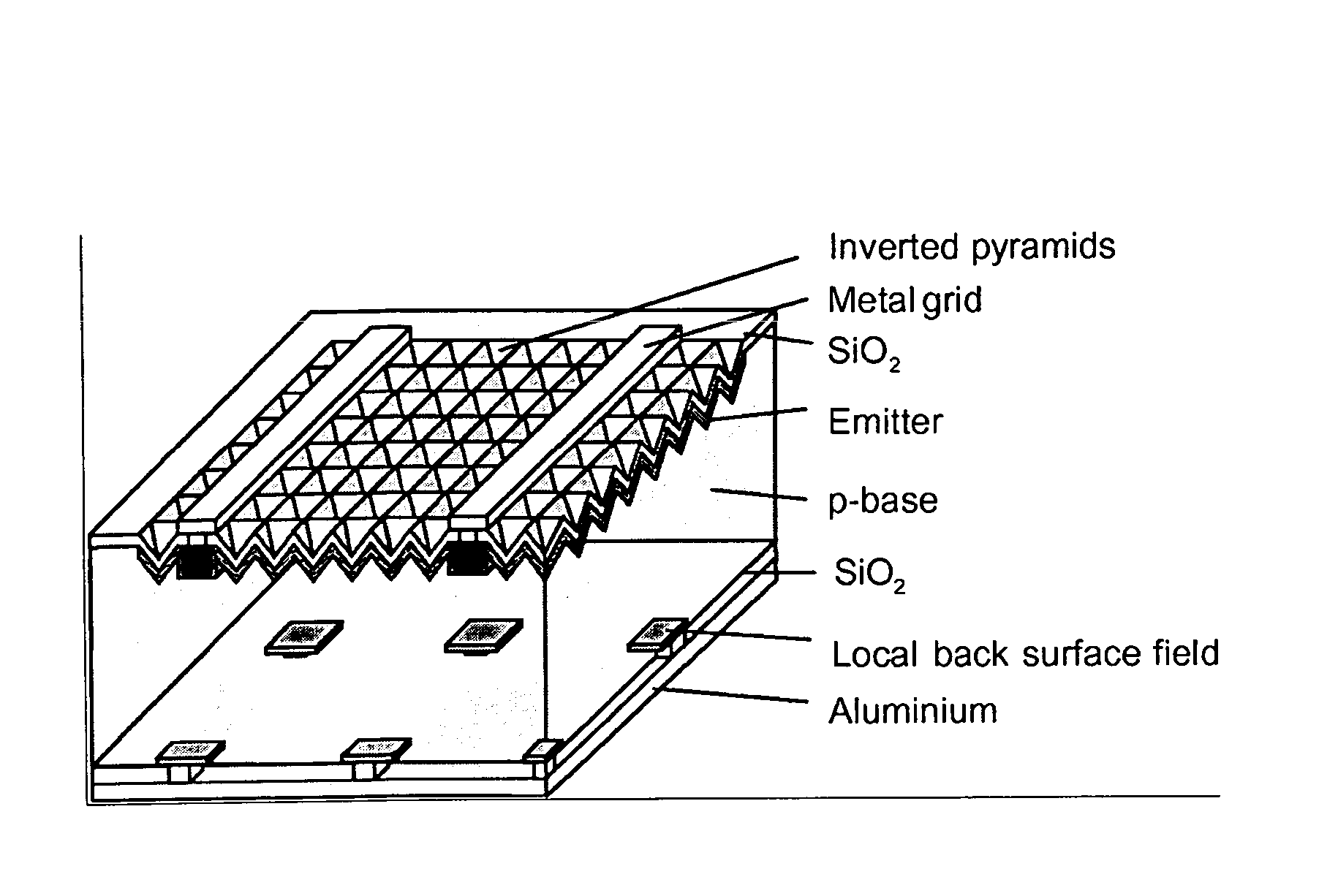
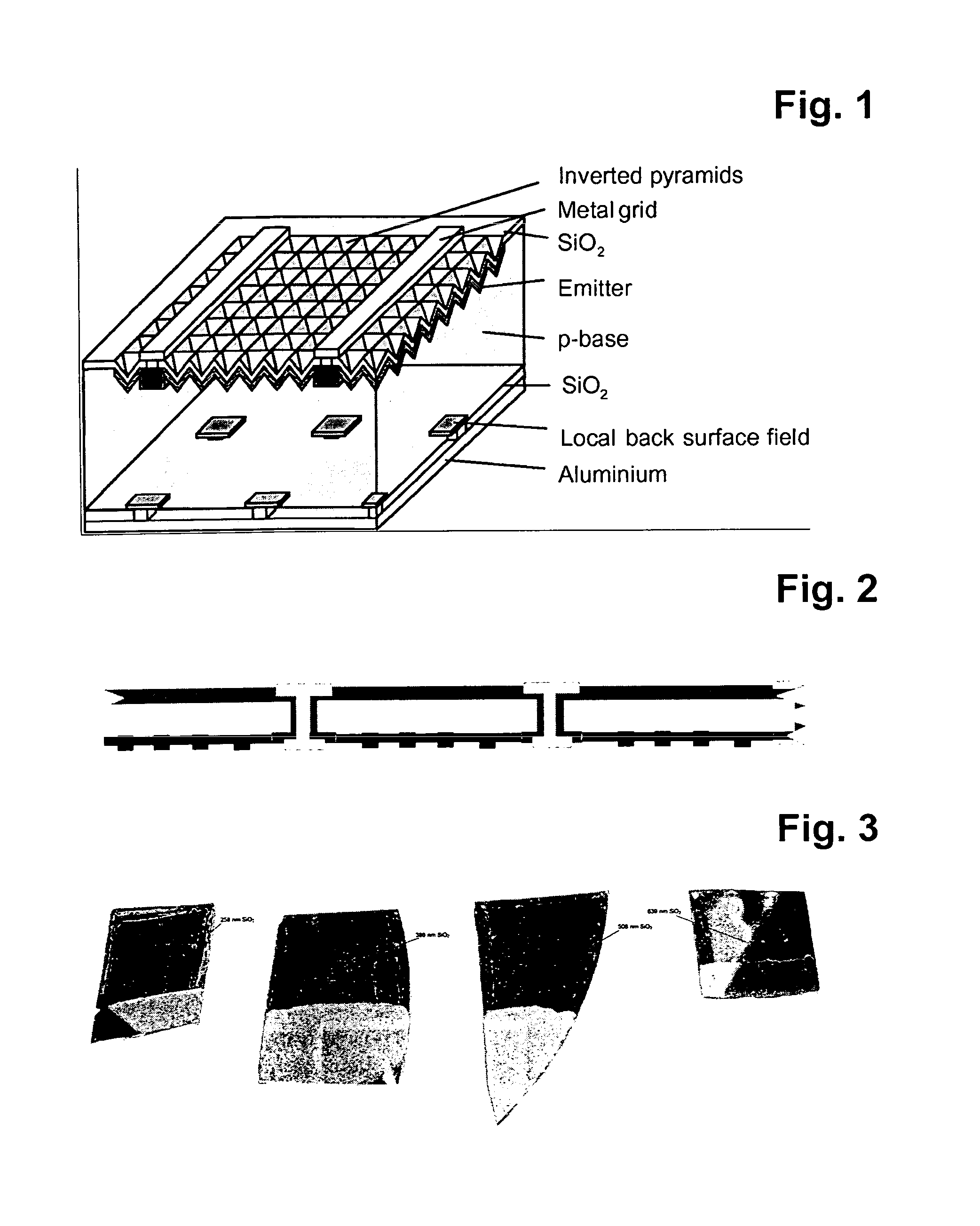
[0070]In order to investigate a possible barrier action of SiO2, 4 wafer pieces (Cz, p-type, polished on one side, 10 Ω*cm) are coated with SiO2 in the sol-gel process by spin coating (optionally with multiple coating, if necessary, where each layer is thermally compacted in advance as described in Example 1) and various layer thicknesses, and the sol applied is thermally compacted (30 min at 450° C., as described in Example 1). Half of each wafer is etched free by an HF dip.

[0071]FIG. 3 shows photographs of the wafer pieces before metallisation.

[0072]An aluminium metal paste is subsequently applied to the entire surface of the wafer in a layer thickness of 20 μm by means of a hand coater, and the wafer treated in this way is fired for 100 s in a belt furnace having four zones (T set points: 850 / 800 / 800 / 800° C.). The aluminium paste is subsequently removed by etching with a phosphoric acid (85%) / nitric acid (69%) / acetic acid (100%) mixture (in v / v: 80 / 5 / 5, remainder water). The SiO2...

example 3

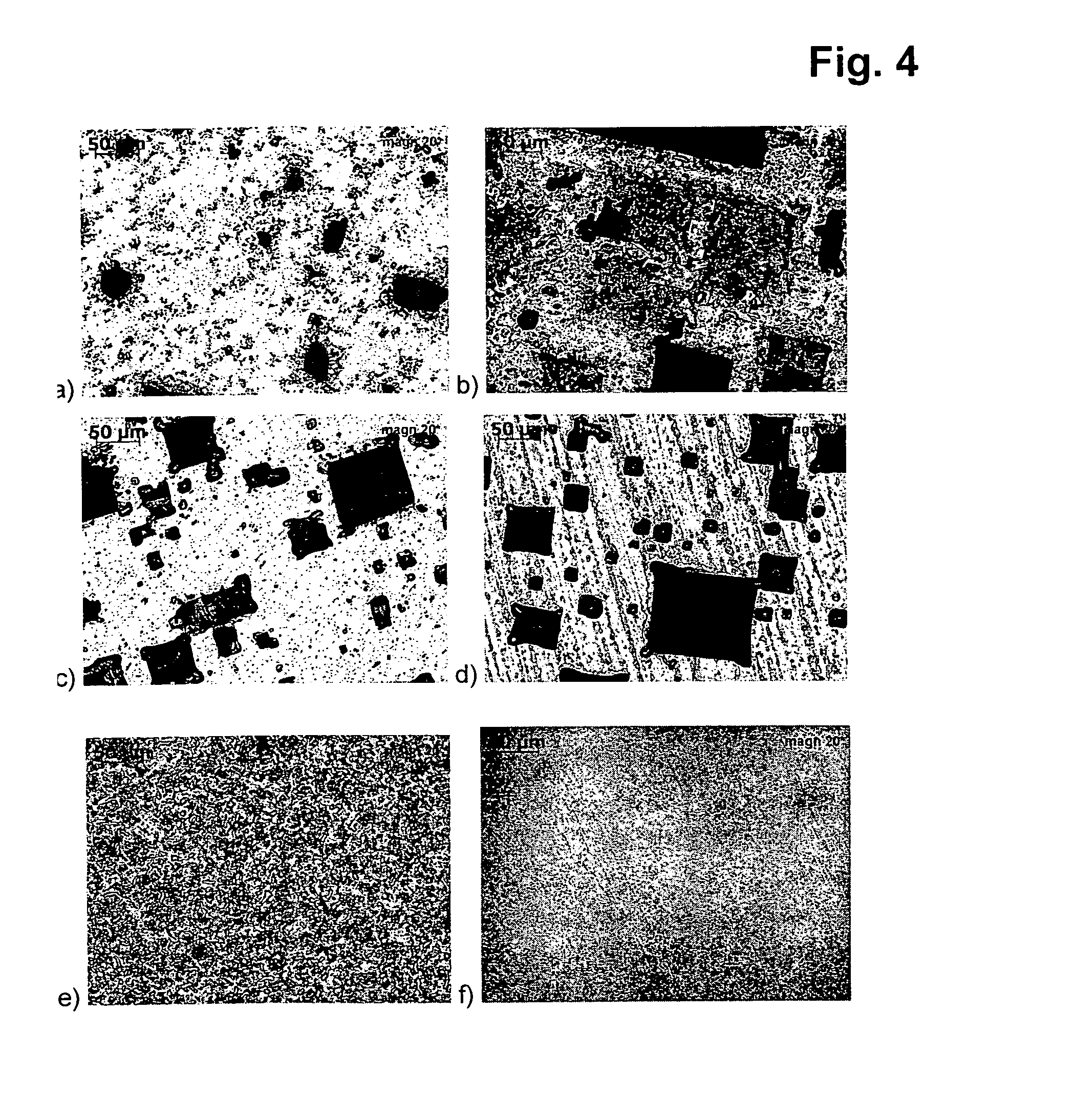
[0077]3 wafer pieces (Cz, p-type, polished on one side, 10 Ω*cm) are coated with a sol-gel-based Al2O3 layer by spin coating to give various layer thicknesses (optionally with multiple coating, if necessary, where each layer is thermally compacted in advance, as described under Example 1). The sol layer is thermally compacted (30 min at 450° C., as described under Example 1), and half of the Al2O3 layer is subsequently removed by etching with dilute HF solution.

[0078]FIG. 5 shows photographs of the wafer pieces before metallisation.

[0079]An aluminium metal paste is subsequently applied to the entire surface of the wafer in a layer thickness of 20 μm by means of a hand coater, and the wafer is fired for 100 s in a belt furnace having four zones (T set points: 850 / 800 / 800 / 800° C.). After the firing process, the aluminium paste is removed by etching with a phosphoric acid (85%) / nitric acid (69%) / acetic acid (100%) mixture (in v / v: 80 / 5 / 5, remainder water). The Al2O3 layer and any paras...


PUM

PropertyMeasurementUnit
thicknessaaaaaaaaaa
thicknessaaaaaaaaaa
temperaturesaaaaaaaaaa

Abstract

The present invention relates to aluminium oxide-based passivation layers which simultaneously act as diffusion barrier for underlying wafer layers against aluminium and other metals. Furthermore, a process and suitable compositions for the production of these layers are described.

Description

[0001]The present invention relates to aluminium oxide-based passivation layers which simultaneously act as diffusion barrier for underlying wafer layers against aluminium and other metals. Furthermore, a process and suitable compositions for the production of these layers are described.[0002]Ever-thinner solar wafers (current thickness 200-180 μm with a strong trend towards 160 μm) are causing ever more-pressing problems in conventional full-area metallisation on the back. On the one hand, the surface recombination speed in the strongly aluminium-doped layer is very high (typically 500-1000 cm / s) and cannot be reduced further as desired by means of the existing conventional technology. The consequence is a lower power output compared with more advanced, but also more expensive concepts, which is principally evident from lower short-circuit currents and reduced open terminal voltage. On the other hand, the full-area metallisation and the requisite firing process for this purpose, wh...

Claims


Application Information

Patent Timeline
Patent Type & Authority Applications(United States)
IPC IPC(8): H01L31/0216
CPCH01L31/02167C23C18/1216C23C18/1254C23C18/1295C23C24/082C23C26/00H01L31/022425H01L31/02245C23C18/12C23C24/08H01L31/18Y02E10/50
Inventor KOEHLER, INGODOLL, OLIVERSTOCKUM, WERNERBARTH, SEBASTIAN
Owner MERCK PATENT GMBH
Why Eureka
Try Eureka