Transistor device and materials for making

Active Publication Date: 2014-01-09
UNIV OF MANCHESTER
View PDF8 Cites 43 Cited by
  • Summary
  • Abstract
  • Description
  • Claims
  • Application Information

AI Technical Summary

Benefits of technology

[0157]To demonstrate the transistor operation, FIG. 7A plots the influence of gate voltage on I. Vg significantly enhances the tunnel current and the changes are strongest at low bias. The field effect is rather gradual for all gate voltages up to ±50V, a limit set by the electrical breakdown of our SiO2 gate dielectric at typically ≈60V. To quantify this behavior, FIG. 7B plots the low-bias tunneling conductivity σT=I/Vb as a function of Vg. The influence of Vg is clearly asymmetric: σT changes by a factor of ≈20 for negative Vg (holes) and by a factor of 6 for positive Vg (electrons). We observed changes up to ≈50 for hole tunneling in other devices and always the same asymmetry (fig. S4). Also, the I-V curves of the devices showed little change between room and liquid-helium temperatures, as expected for Δ>>thermal energy.
[0158]To analyze the observed behavior of σT (Vg), we modeled the zero-bias conductivity by using the relation σT∝DoSB(Vg)×DoST(Vg)×T(Vg), where the indices refer to the two graphene layers and T(Vg) is the transmission coefficient through the hBN barrier. The resulting curve shown in FIG. 7B explains qualitatively the main features in the measured data, using self-consistently the same tunneling parameters m

Problems solved by technology

A major challenge in research on graphene is to find innovative ways to exploit its remarkable properties.
Of particular interest is the possibility of using graphene as an alternative to silicon-based electronics but the absence of an energy gap presents a severe obstacle in achieving low power dissipation in the OFF state.
The performance of graphene-based field effect transistors (FETs) has been hampered by graphene's metallic conductivity at the neutrality point (NP) and the unimpeded electron transp

Method used


Image

  • Transistor device and materials for making
  • Transistor device and materials for making
  • Transistor device and materials for making

Examples


example 2

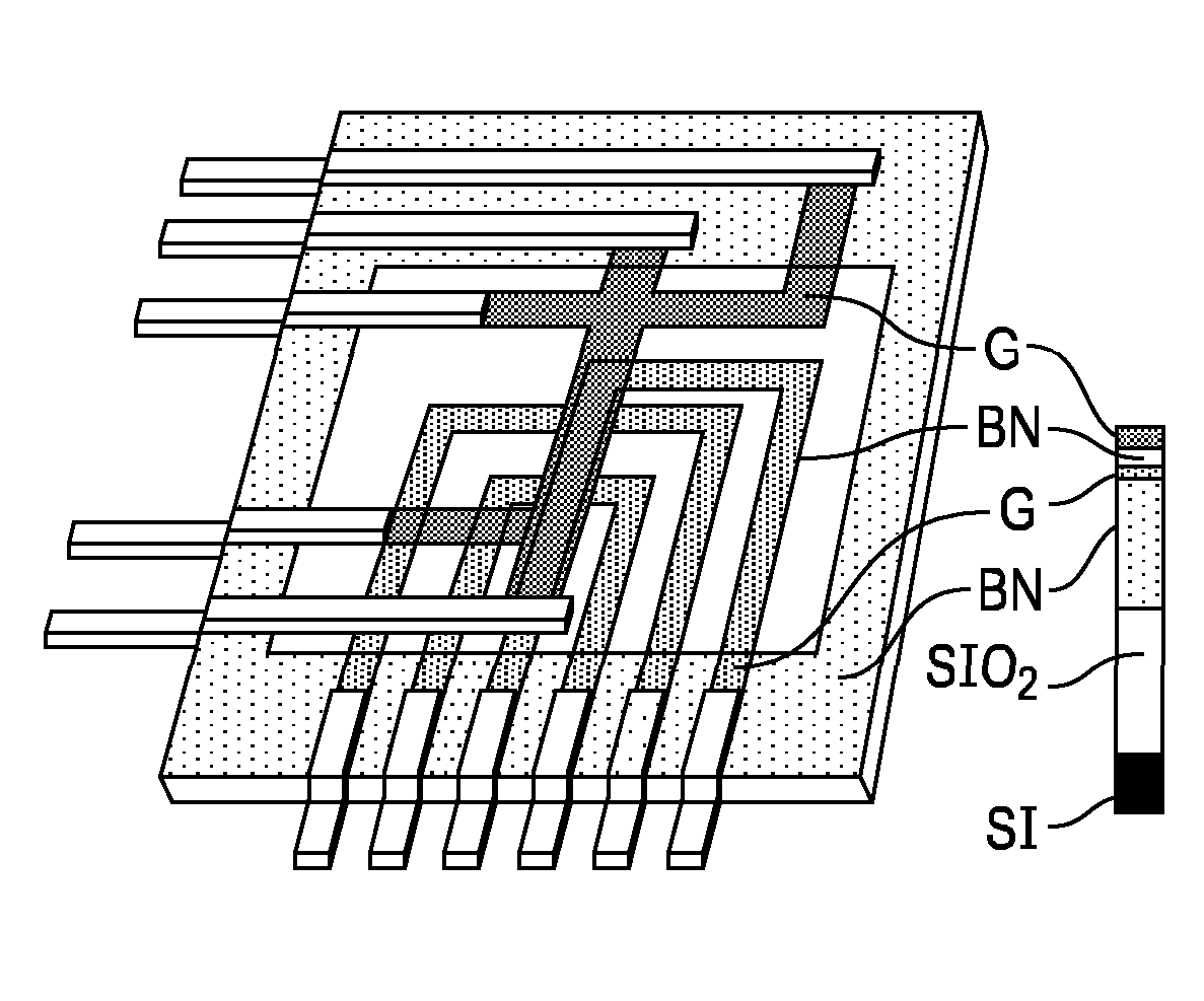
Penetration of Electric Field Through the Graphene Electrode

[0165]Consider the geometry shown in FIG. 5A above. The external electric field between the Si and bottom graphene electrodes, which are separated by distance D, is Fg=Vg / D (dielectric constants for both SiO2 and hBN are similar and, for simplicity, we assume them both equal toe). The electric field Fb between GrB and GrT and the induced carrier densities in the graphene plates nT and nB are related by the equations

∈(Fb−Fg)=4πnBe

−∈Fb=4πnTe

A bias voltage Vb between the two graphene electrodes is given by

eVb=eFbd−μ(nT)+μ(nB)

where d is the hBN thickness and μ(n) are the chemical potentials in the corresponding graphene layers. For simplicity, we assume that graphene electrodes are chemically undoped and, therefore, nT=nB=0 in the absence of applied voltages.

[0166]Taking into account the electron-hole symmetry μ(−n)=−μ(n), we obtain the following equation

4π2dɛnT+μ(nT)+μ(nT+ɛFg4π)+eVb=0(S1)

which allows us to determine nT induc...

example 3

Modeling of Our Device Operation

[0169]I-V curves for a tunnel junction are generally described by the expression:

I(V)∝∫dEDoSB(E)DoST(E−eV)T(E)[f(E−eV)−f(E)]  (S2)

where f(E) is the Fermi distribution function. At low temperatures the difference of the Fermi functions restricts the relevant energy E integral to μ0. The above formula assumes that there is no in-plane momentum conservation, which is most likely to be the case of realistic graphene-hBN interfaces. There are several possible mechanisms for elastic scattering at the interface and, in particular, unavoidable fluctuations of the mass term due to the lattice mismatch. Note that elastic tunneling is forbidden between two 2D systems if in-plane momentum is conserved.

[0170]If the tunneling conductance per channel is much smaller than the conductivity quantum e21 h (as in our case) the transmission probability T is exponentially small and depends strongly on the energy E of tunneling electrons,

T(E)=A(E)exp[−W(E)]  (S3)

where A is ...

example 4

Layered Versus Isotropic Barrier

[0176]In the description above, we have chosen for the sake of brevity to ignore the fact that our tunnel barriers are made from a strongly layered material. This simplification allowed us to refer to the standard tunneling theory. However, the assumption can be justified further by the fact that, for our device parameters, we have found no difference between the I-V characteristics calculated for the layered and isotropic materials and, therefore, we cannot distinguish between the two cases.

[0177]To illustrate the indifference to the layered structure of our tunnel barrier, FIG. 11 shows experimental I-V curves for two devices and compares them with the behavior expected for layered and isotropic cases. No major difference can be seen, except at low bias in FIG. 11A. The exact shape of experimental curves at low bias varies from sample to sample (cf. FIGS. 11A& B) and, hence, we do not discuss the difference.

[0178]FIG. 11 shows the tunneling I-V char...


PUM


Abstract

This application relates to graphene based heterostructures and transistor devices comprising graphene. The hetero-structures comprise i) a first graphene layer; ii) a spacer layer and iii) a third graphene. The transistors comprise (i) an electrode, the electrode comprising a graphene layer, and (ii) an insulating barrier layer.

Description

[0001]This invention generally relates to transistor devices comprising an electrode, the electrode comprising a graphene layer. The invention also relates to graphene heterostructures from which said devices can be made. In particular, the present invention relates to transistors comprising (i) an electrode, the electrode comprising a graphene layer, and (ii) an insulating barrier layer. In one variant, the insulating barrier layer may comprise at least one boron nitride (BN) layer and / or at least one molybdenum disulfide layer. Thus, in some embodiments the transistors of the present invention may comprise a boron-nitride / graphene heterostructure. However, it is expected that when a transistor according to the invention is produced on a large scale it is likely that the insulating barrier will be made of a different material such as those described below.[0002]A major challenge in research on graphene is to find innovative ways to exploit its remarkable properties. Of particular i...

Claims


Application Information

Patent Timeline
IPC IPC(8): H01L29/775H01L21/02H01L29/06
CPCH01L29/775H01L29/06H01L21/02104H01L29/1606H01L29/2003H01L29/267H01L29/41725H01L29/51H01L29/778
Inventor GEIM, ANDRENOVOSELOV, KOSTYAGORBACHEV, ROMANPONOMARENKO, LEONIDBRITNELL, L.
Owner UNIV OF MANCHESTER
Why Eureka
Try Eureka