
Silicon-based proton exchange membrane (PEM) and method of making a silicon-based PEM

Inactive Publication Date: 2014-01-23
SHANNON MONA
View PDF9 Cites 5 Cited by
  • Summary
  • Abstract
  • Description
  • Claims
  • Application Information

AI Technical Summary

Benefits of technology

The patent introduces a special membrane that allows protons to pass through it without changing its shape or size. This membrane is made using silicon and can be used to create membrane electrode assemblies (MEAs) and micro-electrode arrays (MEAs) for use in fuel cells. This technology helps to improve the performance of fuel cells by ensuring constant and efficient proton conductivity regardless of humidity levels.

Problems solved by technology

Although advancements in lithium-ion battery technology in recent years have provided higher power devices, this progress has not kept pace with the portable technologies, leaving a so-called power gap that is widely expected to grow in coming years.
However, efforts to harvest this high energy density have been hampered by issues concerning MFCs fabrication, performance, reliability, size, and cost.
Proton exchange membrane (PEM) fuel cells could have applications in energy conversion and energy storage but their development has been impeded by problems with the membrane electrode assembly (MEA).
At the heart of the issues is the use of polymer membranes (e.g., Nafion), which exhibit both low conductivity at low humidity and a large volumetric size change with humidity that is a major source of failure and integration difficulties.

Method used


Image

  • Silicon-based proton exchange membrane (PEM) and method of making a silicon-based PEM
  • Silicon-based proton exchange membrane (PEM) and method of making a silicon-based PEM
  • Silicon-based proton exchange membrane (PEM) and method of making a silicon-based PEM

Examples


example 1

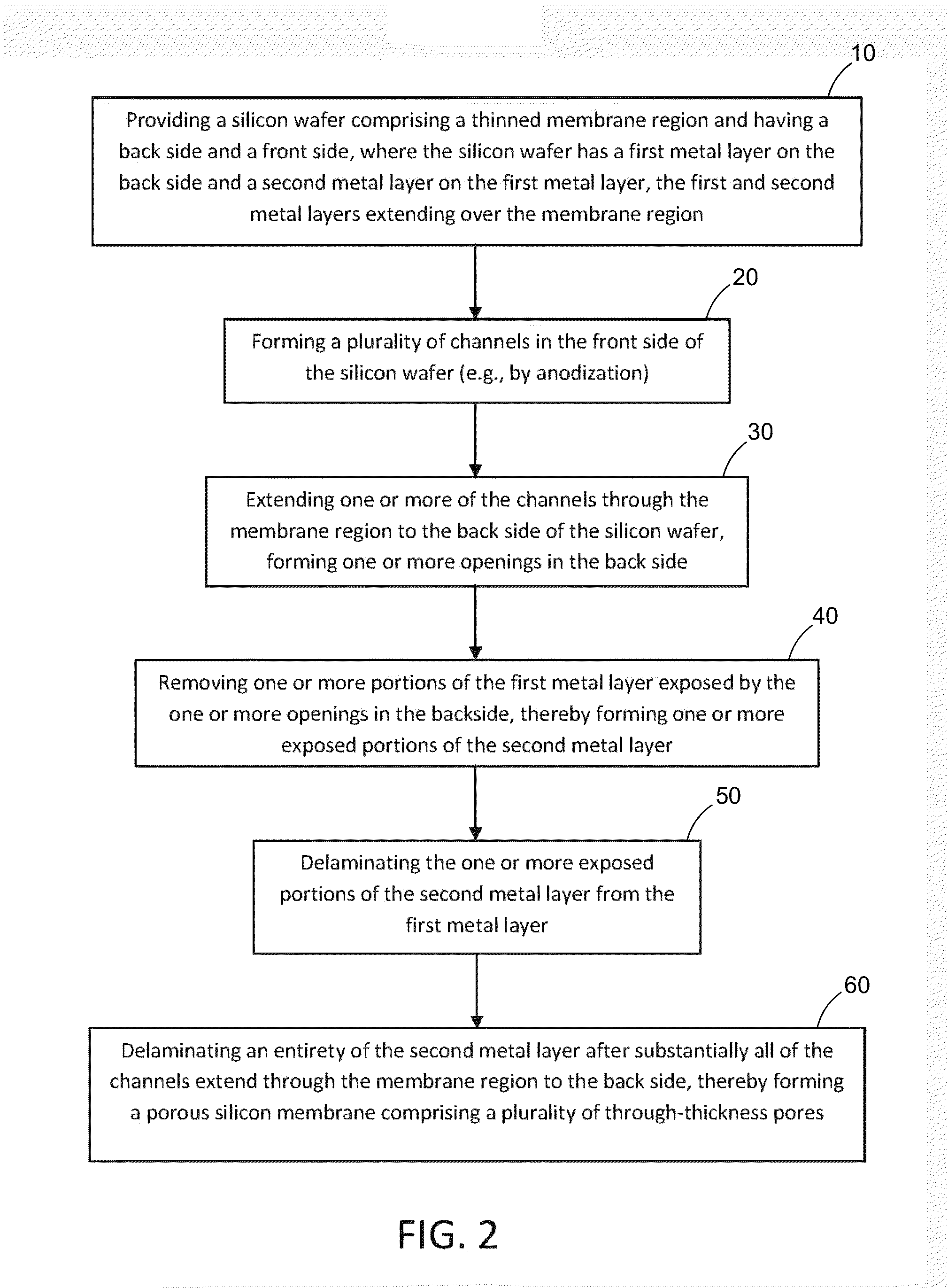
Fabrication of Porous Silicon Membrane

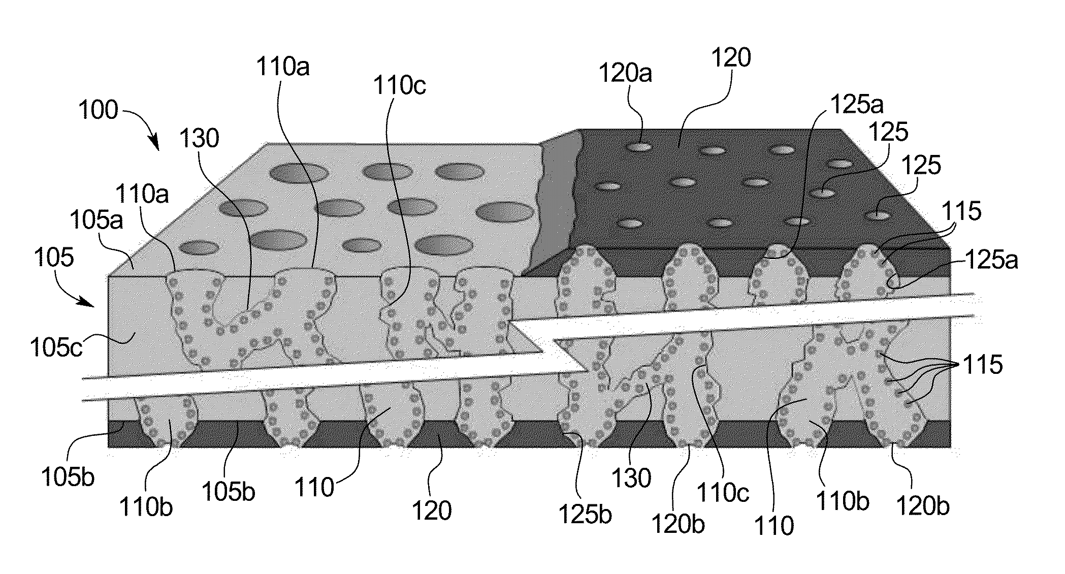
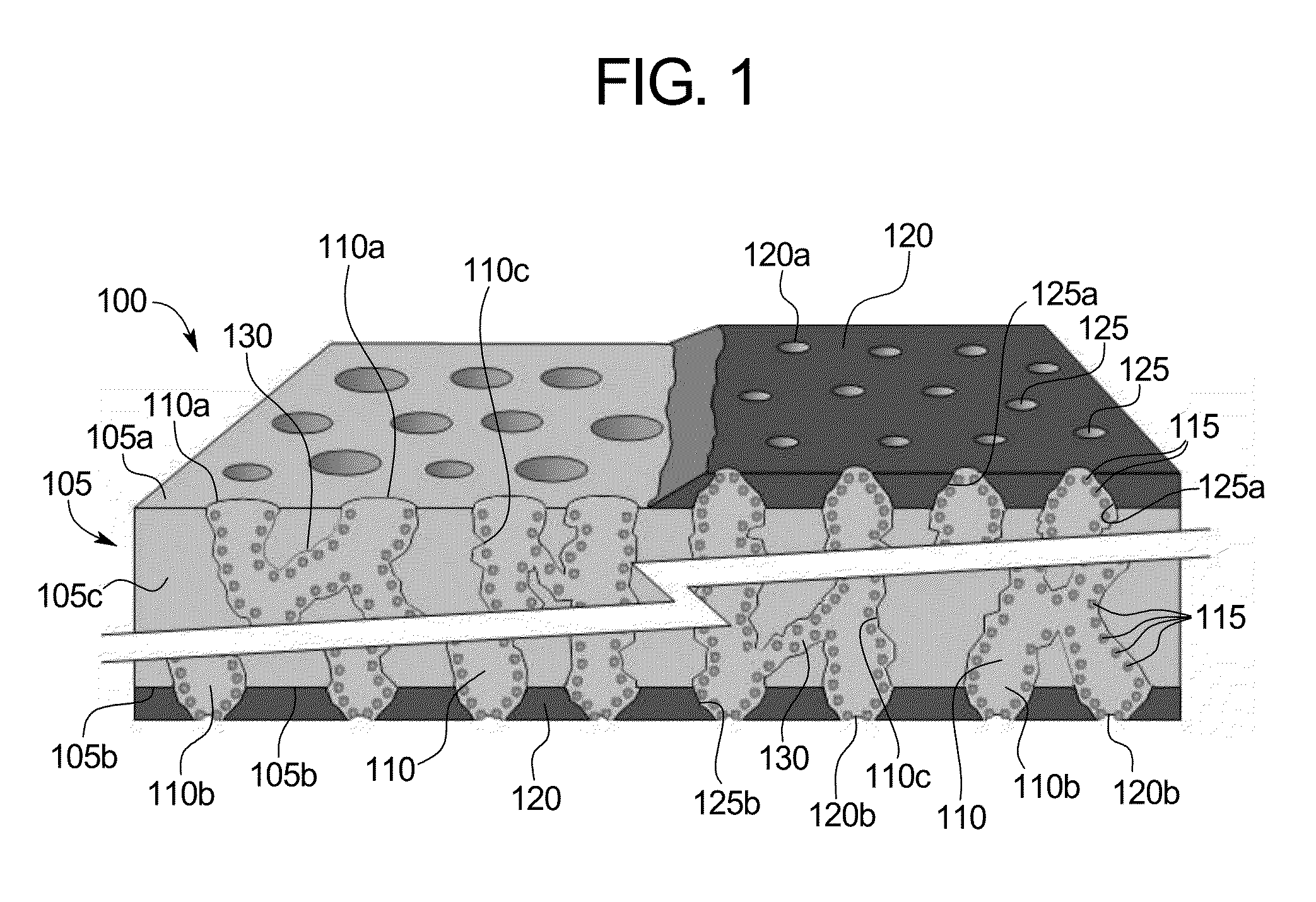
[0035]Fabrication of the silicon membranes may begin with KOH etching of a p-doped silicon wafer. A 0.8 μm thick LPCVD nitride layer is used as a protection mask in KOH solution. First, the nitride layer on the backside of the membrane is patterned and etched using a Freon plasma. The exposed silicon areas are then etched in KOH until a membrane thickness of 24±2 μm is reached. The nitride layer on the frontside of the membrane is subsequently patterned and etched to expose silicon. In membranes with an additional metal layer on the frontside, the patterning step is followed by wet etching of the metal layer and then Freon plasma etching of the nitride layer.

[0036]Prior to anodizing the silicon wafer, metal films may be deposited on the back side by using a magnetron sputtering system at 5×10⁻² Torr pressure and 300 W DC power in argon gas. The resulting backside Cr / Au layer may be wired directly to the anode electrode to provide an electrical ...

example 2

Hydroxylation of Pore Walls

[0037]After the anodization process, the membrane may be left in de-ionized (DI) water for a few hours to clean the anodization electrolyte from the pores. As the Fourier Transfer Infrared (FTIR) spectra of the membrane (FIG. 4(a)) suggests, the pore wall is covered with SiHx (x=1-3) hydrophobic surface species (the absorption bands were assigned by Glass et al., Surf. Sci. 348 (1996) 325-334). To successfully conduct silane-based self-assembly within the membrane, the surfaces of the pores may be converted to hydrated silica. This can be achieved in two steps. First, the membrane may be partially oxidized at low temperature (300° C.) in an oxygen environment (e.g., O2 furnace). Although close to 600° C. may be required to desorb surface hydride species, processing at such a temperature level is not practical due to significant changes in membrane morphology and membrane fracturing. The morphology of porous silicon is known to change at temperatures above ...

example 3

Functionalization of Pore Walls

[0038]Due to the large surface area and high aspect ratio of the pores, a reactor was constructed (FIG. 5(a)) to continuously supply an approximately 1 mM solution of MPTMS to one end of the pores and extract the solvent from the opposite end.

[0039]The membrane die is installed within a fixture between the top and bottom compartments of the functionalization setup. This arrangement allows extraction of the depleted solvent from the bottom of the membrane pores continuously while the solute-rich solvent is supplied over the membrane. A typical process run involves evacuating the chamber and purging with helium multiple times to remove condensed water from the pores. Excess water results in self-polymerization of the MPTMS molecules and clogging of the pores (note that surface adsorbed water remains on the surface). Then, MPTMS in benzene solution is supplied to the solution reservoir on top of the membrane. While the top chamber was charged with helium ...


PUM

PropertyMeasurementUnit
Thicknessaaaaaaaaaa
Thicknessaaaaaaaaaa
Thicknessaaaaaaaaaa

Abstract

A silicon-based proton exchange membrane for a membrane electrode assembly comprises a silicon wafer including a back side, a front side, and a membrane region therebetween, where the membrane region includes a plurality of channels extending from openings in the front side of the silicon wafer through the membrane region to openings in the back side of the silicon wafer. Walls of the channels include active sites to which a molecular species may be attached. Each of the front side and the back side of the silicon wafer includes a porous capping layer thereon. The capping layer comprises a plurality of through-thickness apertures contiguous with at least a portion of the channels of the membrane region.

Description

RELATED APPLICATION[0001]The present patent document claims the benefit of the filing date under 35 U.S.C. 119(e) of U.S. Provisional Patent Application Ser. No. 61 / 410,600, filed on Nov. 5, 2010, which is hereby incorporated by reference in its entirety.FEDERALLY SPONSORED RESEARCH OR DEVELOPMENT[0002]This subject matter of this application has been funded by the Defense Advanced Research Projects Agency (DARPA) under contract number DST 2007-0299513-000-1 and banner / UFAS no. 1-493673-687001-191100. The U.S. Government has certain rights in this invention.TECHNICAL FIELD[0003]This disclosure is related generally to proton exchange membranes (PEMs) and more particularly to silicon-based PEMs.BACKGROUND[0004]The ever increasing demand for powering portable devices has generated a worldwide effort for development of high energy density power sources. Although advancements in lithium-ion battery technology in recent years have provided higher power devices, this progress has not kept p...

Claims


Application Information

Patent Timeline
IPC IPC(8): H01M8/10
CPCH01M8/1016B01D67/0034B01D71/027B01D69/12B01D71/022Y02P70/50Y02E60/50B01D71/0221B01D71/02232B01D71/02231
Inventor MOGHADDAM, SAEEDSHANNON, MARK A.BRINKER, CHARLES JEFFREY
Owner SHANNON MONA
Features
  • Generate Ideas
  • Intellectual Property
  • Life Sciences
  • Materials
  • Tech Scout
  • Unparalleled Data Quality
  • Higher Quality Content
  • 60% Fewer Hallucinations
Learn More