
Semiconductor device and program

Inactive Publication Date: 2014-06-05
SEMICON ENERGY LAB CO LTD
View PDF9 Cites 35 Cited by
  • Summary
  • Abstract
  • Description
  • Claims
  • Application Information

AI Technical Summary

Benefits of technology

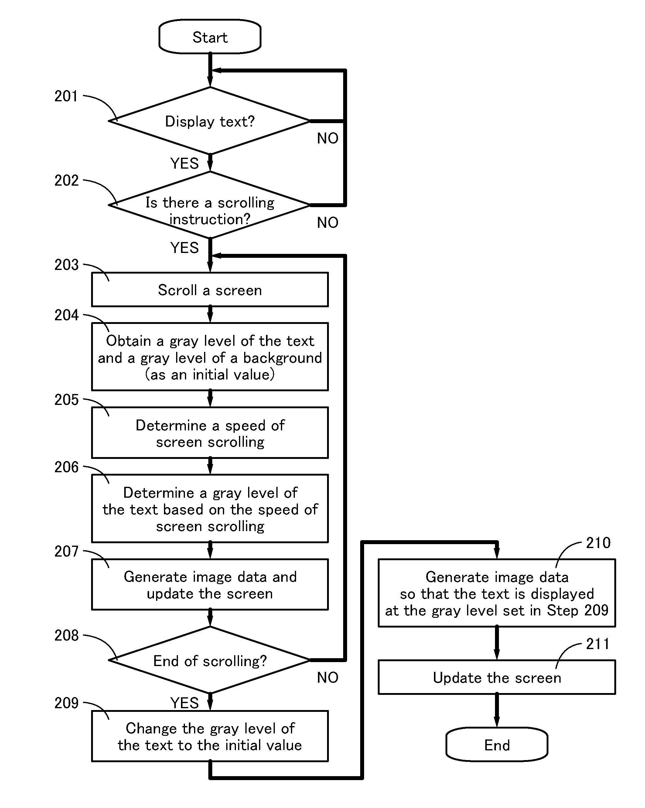
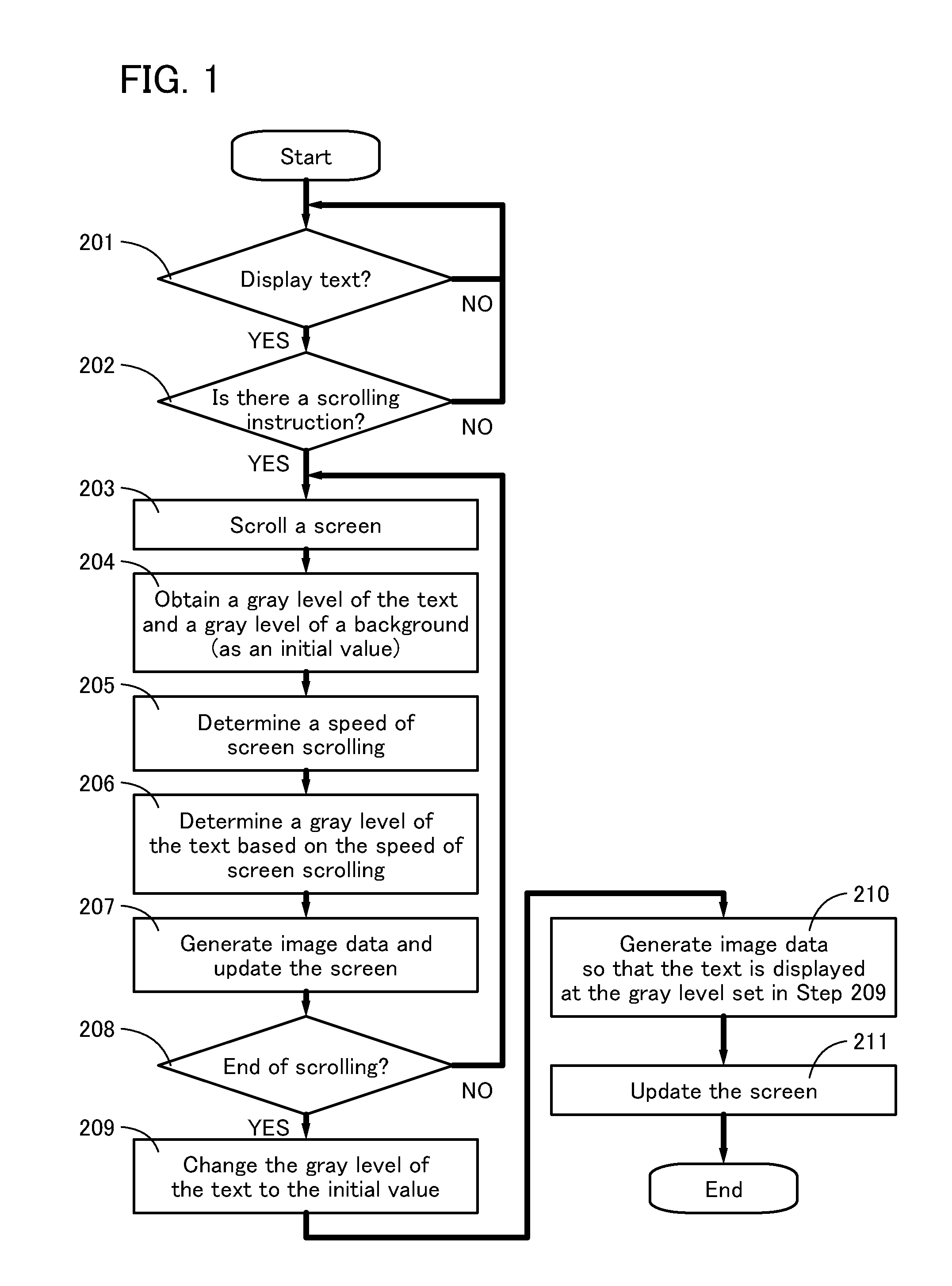
This patent describes a semiconductor device that has several technical functions. First, it provides a display that is more eye-friendly, meaning it reduces eye strain. Second, it consumes less power. Third, it allows for more pixels with a high aperture ratio. Fourth, it is less affected by finger pressure on the screen and screen flicker. Fifth, it can display high-resolution images. Lastly, it has a low drive voltage and off-state current. Additionally, it can be made flexible and used on a bended screen. The patent also describes a program for controlling the display unit, which takes into account the scrolling speed of the screen and reduces the difference between the gray level of text and the background level of text accordingly. Overall, this patent provides a technical solution for creating a semiconductor device that can provide a more comfortable visual experience with reduced eye strain.

Problems solved by technology

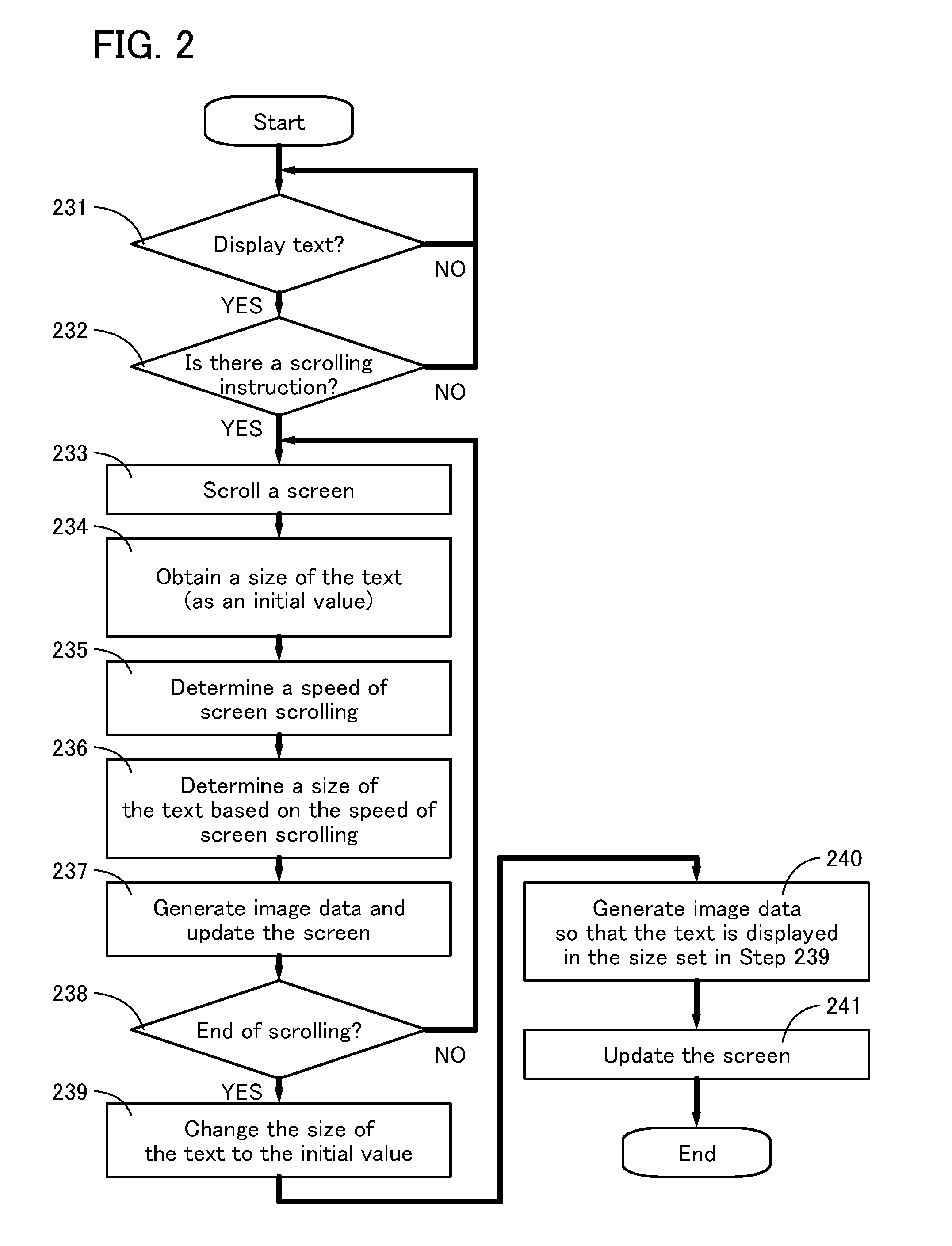
Causes of eye strain due to use of personal computers and the like include intense light from screens, fast movement of text by scrolling, and the like.

Method used


Image

  • Semiconductor device and program
  • Semiconductor device and program
  • Semiconductor device and program

Examples


embodiment 1

[0038]Reading text on a screen of a personal computer or the like causes more eye strain than reading printed text on paper does because it requires a completely different way of using eyes. A display device requires scrolling to move displayed text on a screen, and therefore, text is moved rapidly. However, a user stares at a screen unconsciously in an attempt to read fast-moving text, and this causes eye strain.

[0039]In view of this explanation, a semiconductor device including a display portion capable of displaying text with less eye strain is described in this embodiment.

[0040]Methods for quantifying eye fatigue have been studied. For example, critical flicker (fusion) frequency (CFF) is known as an indicator for evaluating nervous fatigue. Further, accommodation time, accommodation near point, and the like are known as indicators for evaluating muscular fatigue.

[0041]Others methods for evaluating eye fatigue include electroencephalography, thermography, counting the number of ...

embodiment 2

[0119]In this embodiment, as in Embodiment 1, technology related to a display device for reducing eye strain is described.

[0120]Blue light refers to high-energy light (wavelength: 360 nm to 495 nm) in the visible range. Blue light reaches the retina in the eye without being absorbed by the cornea or the lens, and therefore causes damage to the retina or the optic nerve. In addition, exposure to blue light late at night causes disturbance of the circadian rhythm. The danger from blue light lies in the low visibility of light in that wavelength range to human eyes. Even when exposed to intense blue light, humans cannot be aware of it and therefore damage is easily accumulated.

[0121]Blue light is short-wavelength light and is thus more likely to be scattered than long-wavelength light (such as green light or red light). In addition, blue light is easily refracted and thus has a short focal length. When a user keeps looking at a screen of a display device for a long time while much blue...

embodiment 3

[0155]In this embodiment, transistors in the display module 122 (see FIGS. 4B to 4D, FIGS. 5A and 5B, FIG. 6, and the like) of the display unit 120 are described.

[0156]As a semiconductor for transistors used in the display module 122, single crystal silicon, polycrystalline silicon, microcrystalline silicon, amorphous silicon, or an oxide semiconductor can be used. Transistors formed using an oxide semiconductor are preferable in terms of display performance of the display module 122.

[0157]An oxide semiconductor has a wide energy gap of 3.0 eV or more. A transistor including an oxide semiconductor film obtained by processing the oxide semiconductor under appropriate conditions and by reducing the carrier density sufficiently (hereinafter referred to as “oxide semiconductor transistor”, and other semiconductors are also similar) can have much lower leakage current (off-state current) between a source and a drain in an off state than a conventional silicon transistor.

[0158]Accordingly...


PUM


Abstract

A semiconductor device having an eye-friendly display function is provided. When a display portion displays text, a difference between a gray level of the text and a gray level of a background of the text is reduced depending on a scrolling speed of a screen of the display portion. In other words, during fast scrolling, text visibility is lowered by bringing the gray level of the text closer to the gray level of the background. This can prevent a user from following the text with eyes at the time of fast scrolling, thereby eliminating unnecessary movement of eye muscles and reducing stimuli to the optic nerve. In this manner, eye strain can be reduced.

Description

BACKGROUND OF THE INVENTION[0001]1. Field of the Invention[0002]The present invention relates to an object, a method, a manufacturing method, a process, a machine, a manufacture, or a composition of matter. The present invention particularly relates to a semiconductor device, a driving method thereof, a manufacturing method thereof, a program for operating the semiconductor device, or the like.[0003]Note that in this specification, a semiconductor device means a circuit including a semiconductor element (e.g., a transistor or a diode) and a device including the circuit. The semiconductor device also means any device that can function by utilizing semiconductor characteristics. For example, an integrated circuit, a chip including an integrated circuit, a display device, a light-emitting device, a lighting device, and an electronic device are all semiconductor devices.[0004]2. Description of the Related Art[0005]With the development of information technology (IT), IT devices such as p...

Claims


Application Information

Patent Timeline
IPC IPC(8): G09G5/37G09G5/373G09G5/02
CPCG09G5/37G09G5/373G09G5/02G09G3/2007G09G5/14G09G5/32G09G5/34G09G2320/0261G09G2340/0435G09G2380/14
Inventor IWAKI, YUJI
Owner SEMICON ENERGY LAB CO LTD
Learn More