Photoelectric conversion element and method of using the same, image sensor, and optical sensor

a technology of photoelectric conversion and image sensor, applied in the field of photoelectric conversion element and a method of using the same, an image sensor, and an optical sensor, can solve the problems of poor light use efficiency, decrease in aperture ratio, and decrease in light collection efficiency, and achieve low dark current characteristics, high photoelectric conversion efficiency, and high productivity

Active Publication Date: 2014-06-12
FUJIFILM CORP
View PDF3 Cites 24 Cited by
  • Summary
  • Abstract
  • Description
  • Claims
  • Application Information

AI Technical Summary

Benefits of technology

[0021]The invention can provide a photoelectric conversion element which exhibits high photoelectric conversion efficiency and low dark current characteristics even in cases where heating treatment is performed, and which is capable of being manufactured with high productivity.

Problems solved by technology

The single-plate solid-state image sensor does not use light which did not pass through the color filters and hence suffers from poor light use efficiency.
In recent years, the pixel size is decreasing with a view to increasing the number of pixels and there arise problems such as a decrease in aperture ratio and a decrease in light collection efficiency.

Method used


Image

  • Photoelectric conversion element and method of using the same, image sensor, and optical sensor
  • Photoelectric conversion element and method of using the same, image sensor, and optical sensor
  • Photoelectric conversion element and method of using the same, image sensor, and optical sensor

Examples


example 1-1

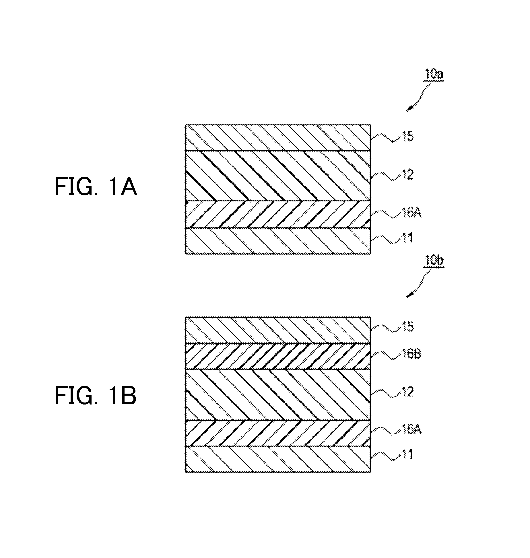
[0258]A photoelectric conversion element having the form of FIG. 1A was prepared. The photoelectric conversion element includes the lower electrode 11, the electron-blocking layer 16A, the photoelectric conversion layer 12 and the upper electrode 15. In other words, an amorphous ITO film with a thickness of 30 nm was formed on a glass substrate by sputtering and used as the lower electrode, and Compound (B-1) was then deposited to a thickness of 100 nm by vacuum heating vapor deposition to form the electron-blocking layer. Compound (A-1) (photoelectric conversion dye) (vapor deposition rate: 0.4 angstrom / s (0.4×10⁻¹⁰ m / s) and fullerene (C60) were further co-deposited on the electron-blocking layer by vacuum heating vapor deposition to thicknesses, in terms of the single layer, of 100 nm and 300 nm, respectively, while controlling the temperature of the substrate to 25° C., thereby forming the photoelectric conversion layer. Amorphous ITO was further deposited for the upper electrode...

examples 1-2 to 1-143

and Comparative Examples 1-1 to 1-80

[0259]The procedure of Example 1-1 was repeated except that Compound (B-1) used for the electron-blocking layer and Compound (A-1) used for the photoelectric conversion layer which were used in Example 1-1 were changed as shown in Table 1, thereby preparing photoelectric conversion elements.

examples 1-144 to 1-234

and Comparative Examples 1-81 to 1-95

[0260]The procedure of Example 1-1 was repeated except that the vapor deposition rate of the photoelectric conversion dye was set to 2.0 angstroms / s (2.0×10⁻¹⁰ m / s) and Compound (B-1) used for the electron-blocking layer and Compound (A-1) used for the photoelectric conversion layer which were used in Example 1-1 were changed as shown in Table 1, thereby preparing photoelectric conversion elements.

[0261]The structural formulae of Illustrative Compounds used in Examples (materials for forming the electron-blocking layer and materials for forming the photoelectric conversion layer) are shown below.

[Evaluation: Evaluation of Voltage Application]

[0262]It was confirmed that, as a result of application of a voltage to the lower electrode and the upper electrode of each of the resulting elements so that the electric field intensity reaches 2.5×10⁵ V / cm, every element shows a dark current of 100 nA / cm2 or less in a dark place but a current of 10 μA / cm2 o...


PUM

PropertyMeasurementUnit
Tgaaaaaaaaaa
vapor deposition rateaaaaaaaaaa
heat resistanceaaaaaaaaaa

Abstract

A photoelectric conversion element includes a transparent conductive film, a conductive film, and a photoelectric conversion layer and an electron-blocking layer disposed between the transparent conductive film and the conductive film. The photoelectric conversion layer includes a condensed polycyclic hydrocarbon which contains at least 5 benzene rings, of which a total number of rings is 7 or more and which contains no carbonyl group. The electron-blocking layer includes a compound A having a residue after removal of at least one group of Ra1 to Ra9 from a compound represented by general formula (A) and having a glass transition point (Tg) of 200° C. or more. The photoelectric conversion element exhibits high photoelectric conversion efficiency and low dark current characteristics even after heating treatment, and can be manufactured with high productivity.

Description

CROSS REFERENCE TO RELATED APPLICATIONS[0001]This application is a continuation application of International Application PCT / JP2012 / 069349 filed on Jul. 30, 2012, which claims priority under 35 U.S.C. 119(a) to Application No. 2011-178047 filed in Japan on Aug. 16, 2011, all of which are hereby expressly incorporated by reference into the present application.BACKGROUND OF THE INVENTION[0002]The present invention relates to a photoelectric conversion element and a method of using the same, an image sensor, and an optical sensor.[0003]A conventional optical sensor is a device having photodiodes (PDs) formed in a semiconductor substrate made of, for example, silicon (Si) and a planar solid-state image sensor in which PDs are two-dimensionally arranged to read out signal charges generated in the respective PDs is widely used as the solid-state image sensor.[0004]The structure in which color filters for transmitting light having specific wavelengths therethrough are disposed on the light...

Claims


Application Information

Patent Timeline
Patent Type & Authority Applications(United States)
IPC IPC(8): H01L51/00H01L51/44
CPCH01L51/0056H01L51/44H01L51/0046B82Y10/00C09B3/14C09B3/78C09B57/00C09B57/001Y02E10/549H10K85/211H10K85/624H10K30/353C07F7/08C07F7/10H01L27/146H01L31/10Y02E10/50H10K30/80
Inventor FUKUZAKI, EIJINOMURA, KIMIATSU
Owner FUJIFILM CORP
Why Eureka
Try Eureka