Reflective mask and method for manufacturing same

Active Publication Date: 2014-06-19
TOPPAN PHOTOMASK CO LTD
View PDF1 Cites 16 Cited by
  • Summary
  • Abstract
  • Description
  • Claims
  • Application Information

AI Technical Summary

Benefits of technology

The present invention provides a method for manufacturing an EUV mask with high light-shielding performance. By stripping a multilayered reflective layer, the invention reduces reflection of EUV light near the edge of the mask to almost zero. This results in better accuracy of pattern formation. The invention also provides a reflective mask with a light-shielding frame that lessens the influence of OoB light, is easy to manufacture, and has high light-shielding ability with no remaining multilayer reflective films.

Problems solved by technology

However, the light-shielding frame, disclosed in Patent Literature 1 described above, simply having dug therein an absorption layer and a multilayered reflective layer has the following problem.
Although EUV reflectance can be reduced almost to zero at a large portion of a light-shielding frame 11 shown in FIG. 23, there is a problem where EUV reflectance (903, 904) in the vicinity of the edge of the light-shielding frame becomes even higher than before the light-shielding frame is formed.
Thus, because of the light-shielding frame 11 for reducing EUV reflectance, leakage of reflected EUV light occurs at the edge portion of the light-shielding frame, causing a problem of increased EUV reflectance and reduced light-shielding performance.
In addition, with multiple exposures, there has been a problem of the chip outer circumferential portion being sensitized not only through exposure with EUV light, but also similarly with light other than that of the 13.5 nm band, from vacuum ultraviolet ray range to near infrared ray range referred to as Out of Band light (hereinafter, OoB (Out of Band) light).
Therefore, light with various wavelengths other than that of 13.5 nm are emitted on the resist on the wafer to cause sensitization, leading to adverse influences such as deviation of pattern dimension in the vicinity of the chip boundary area.
However, in the method disclosed in Patent Literature 1 described above, since it is necessary to process a total of 80 layers of different materials of molybdenum (Mo) and silicon (Si) in the dug-in portion of the multilayered reflective layer at the area of the light-shielding frame after creating a mask pattern, the conditions for achieving dry etching has been very complicated.
In addition, apart from etching of the main pattern, since lithography and etching have to be performed in two separate steps, inconvenience of worsened throughput occurs.
Since substances containing chromium (Cr) is abundantly used in the conductive film as main materials, OoB light that has entered from the mask surface passes through the substrate, is reflected at the reverse surface of the conductive film, passes through the substrate again, and returns to the mask surface, causing an inconvenience of having an adverse influence.

Method used


Image

  • Reflective mask and method for manufacturing same
  • Reflective mask and method for manufacturing same
  • Reflective mask and method for manufacturing same

Examples


first embodiment

[0050]In the following, a first embodiment of the present invention will be described with reference to the drawings.

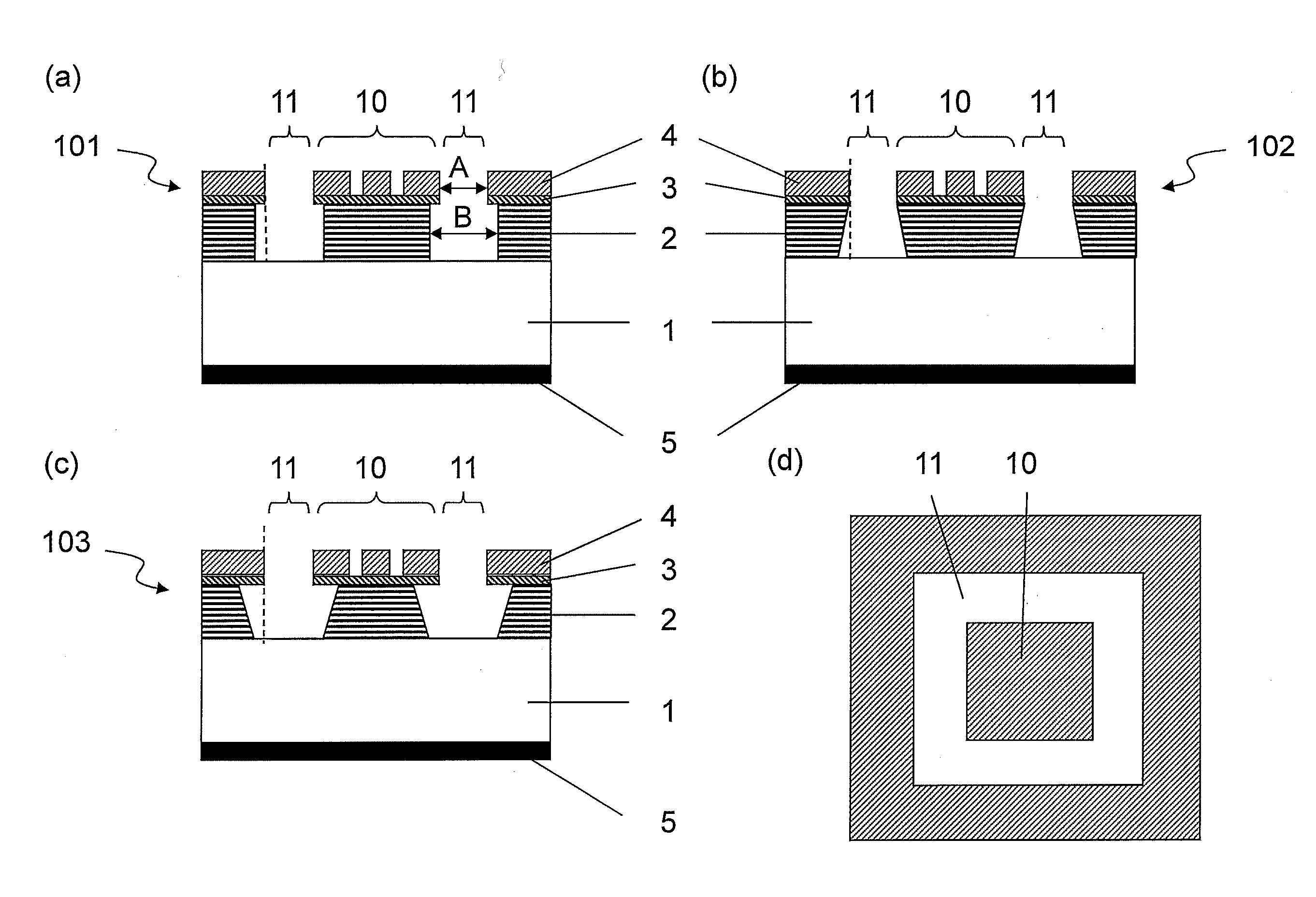
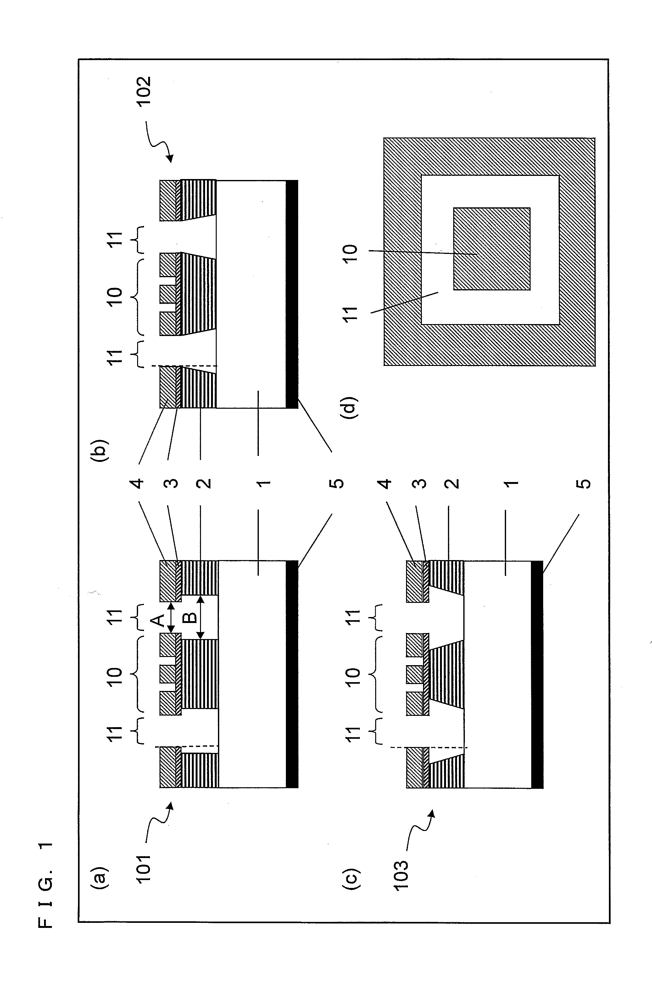
[0051]First, the configuration of reflective masks of the present invention will be described. In FIG. 1, (a), (b), and (c) are outline cross sectional views of structures of the reflective masks of the present invention, and (d) of FIG. 1 is an outline plan (a), (b), and (c) of FIG. 1 viewed from above. Thus the configuration of a reflective mask of the present embodiment may be any of 101, 102, and 103.

[0052]In reflective masks 101, 102, and 103 shown in (a), (b), and (c) of FIG. 1, a multilayered reflective layer 2, a protective layer 3, and an absorption layer 4 are sequentially formed on a surface of a substrate 1. The structure is such that a conductive film 5 is formed on the reverse surface of the substrate. A buffer layer may be included between the protective layer 3 and the absorption layer 4. The buffer layer is a layer provided for not damaging the protec...

example 1-1

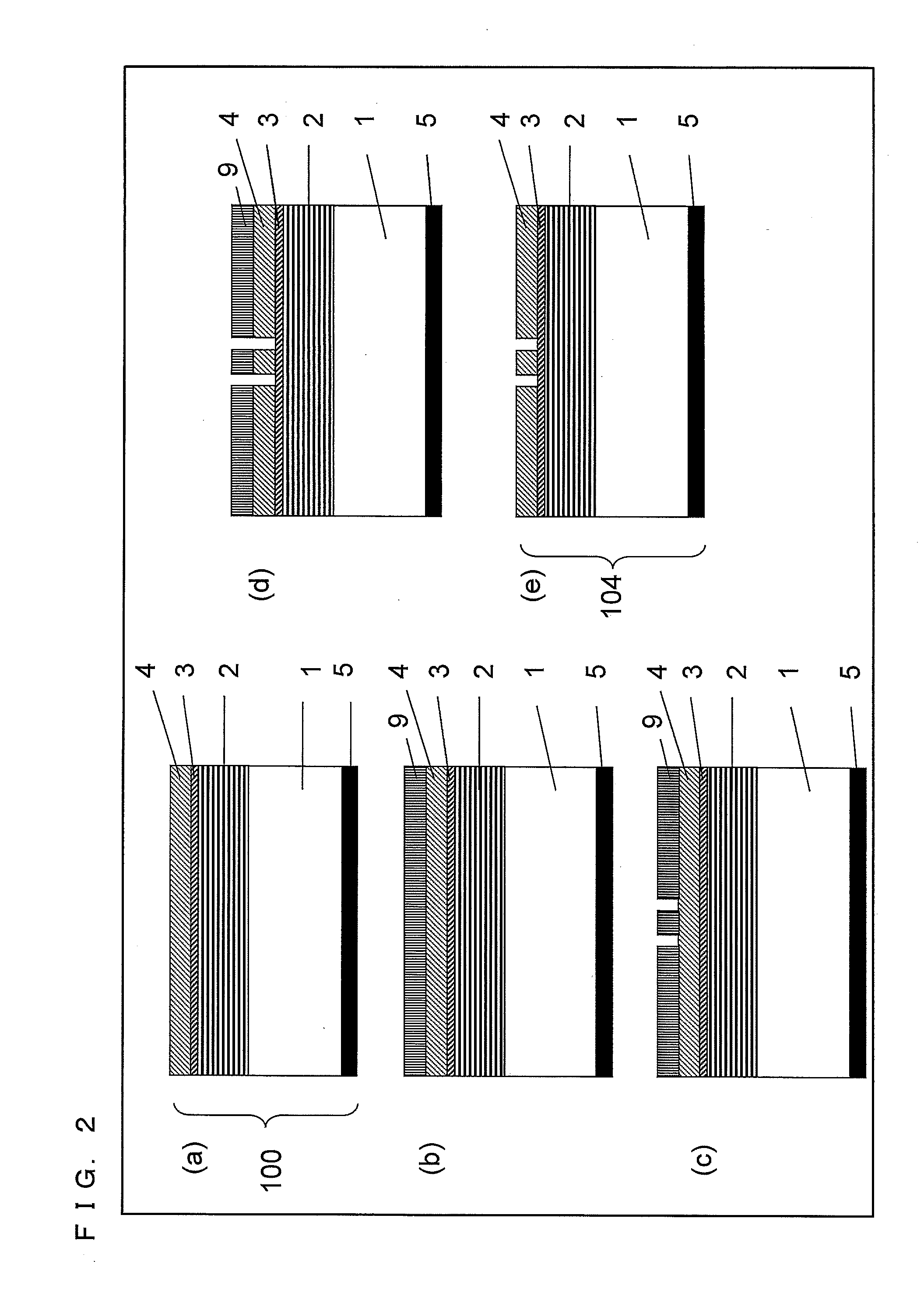
[0069]In the following, a first Example of the method for manufacturing the reflective mask of the present embodiment will be described. First, a reflective mask blank 100 in (a) of FIG. 2 was prepared. The reflective mask blank 100 was formed by sequentially forming, on the substrate 1, the multilayered reflective layer 2 including 40 pairs of Mo and Si and designed such that reflectance against EUV light with a wavelength of 13.5 nm is about 64%, the protective layer 3 of Ru having a thickness of 2.5 nm on the multilayered reflective layer 2, and the absorption layer 4 formed from TaSi having a thickness of 70 nm on the protective layer 3.

[0070]With respect to the reflective mask blank 100, a positive type chemically amplified resist 9 (FEP171: FUJIFILM Electronic Materials) was applied at a film thickness of 300 nm ((b) of FIG. 2), drawing was performed using an electron-beam lithography machine (JBX9000: JEOL Ltd.), post-exposure bake (Post Exposure Bake: PEB) was performed for ...

example 1-2

[0076]A second Example of the method for manufacturing the reflective mask of the present embodiment will be described. The method for forming the main pattern part is a method identical to that of Example 1.

[0077]In the present example, a step was performed to form the light-shielding frame 11 on the pattern area 10 ((a) of FIG. 6) of the reflective mask 104. The i-line resist 29 was applied to the reflective mask 104 with a film thickness of 500 nm ((b) of FIG. 6), and drawing and developing were performed thereon with an i-line drawing machine (ALTA) to form, on the resist portion, a resist pattern having removed therefrom an area that will later be the light-shielding frame 11 ((c) of FIG. 6). The resist pattern had an opening width of 5 mm, and was arranged 3 μm away from the 10 cm×10 cm main pattern area at the central part of the mask.

[0078]Next, the absorption layer was stripped ((d) of FIG. 6) through dry etching with CHF3 plasma (pressure of 15 mTorr, ICP of 300 W, RIE of ...


PUM


Abstract

A reflective mask having a light-shielding frame with high light-shielding performance, and a method for manufacturing thereof. In a reflective mask having a light-shielding frame dug into a multilayered reflective layer, when side etching is performed or processing to obtain a reverse tapered shape is performed only on the multilayered reflective layer, it becomes possible to suppress reflection of EUV light (extreme ultraviolet light) in the vicinity of the edge of the light-shielding frame, provide a reflective mask having high light-shielding ability, and form a transcription pattern with high accuracy.

Description

CROSS-REFERENCE TO RELATED APPLICATIONS[0001]This application is a U.S. continuation application filed under 35 U.S.C. §111 (a), of International Application No. PCT / JP2012 / 005309, filed on Aug. 24, 2012, which claims priority to Japanese Patent Application No. 2011-184186, filed Aug. 25, 2011, Japanese Patent Application No. 2011-213242, filed Sep. 28, 2011, and Japanese Patent Application No. 2011-213243, filed Sep. 28, 2011, the disclosures of which are incorporated by reference.BACKGROUND[0002]1. Field[0003]The present invention relates to a reflective mask and a method for manufacturing the reflective mask; and, in particular, relates to a reflective mask utilized in a semiconductor fabrication device using EUV lithography whose light source is extreme ultraviolet ray (hereinafter, represented as “EUV”), and a method for manufacturing the reflective mask.[0004]2. Description of the Related ArtDescription of EUV Lithography[0005]Associated with miniaturization of semiconductor d...

Claims


Application Information

Patent Timeline
IPC IPC(8): G03F1/24
CPCG03F1/24G03F1/38B82Y10/00B82Y40/00G03F1/22H01L21/027
Inventor FUKUGAMI, NORIHITOSAKATA, YOMATSUI, KAZUAKIWATANABE, GENTA
Owner TOPPAN PHOTOMASK CO LTD
Why Eureka
Try Eureka