Reflective mask blank for EUV lithography, and reflective layer-coated substrate for EUV lithography

Active Publication Date: 2014-08-21
ASAHI GLASS CO LTD
View PDF0 Cites 6 Cited by
  • Summary
  • Abstract
  • Description
  • Claims
  • Application Information

AI Technical Summary

Benefits of technology

[0042]According to the present invention, the incident angle dependence of EUV reflectivity in the reflective layer is improved. At an incident angle θ of EUV light being in a range of −15°≦θ≦+15°, the reflectivity of EUV light is at least 50%, and the fluctuation range of the EUV reflectivity in the above range of θ is within Rmin× 1/10. Thus, the present invention is applicable even to an exposure device with NA of 0.45.
[0043

Problems solved by technology

However, the conventional photolithography method has come close to its limit, while miniaturization of semiconductor devices is being accelerated.
EUV light is likely to be absorbed by all kinds of substances, and the refractive index of substances at such a wavelength is close to 1, whereby it is not possible to use a conventional refractive optical system like photolithography employing visible light or ultraviolet light.
Along with a trend for higher NA (numerical aperture) for an exposure device to be used for EUV lithography, an incident angle dependence of the reflectivity at the mirror surface to be used in a reflective optical system has been problematic (Patent Document 1).
Such an incident angle dependence of the reflectivity becomes problematic also

Method used


Image

  • Reflective mask blank for EUV lithography, and reflective layer-coated substrate for EUV lithography
  • Reflective mask blank for EUV lithography, and reflective layer-coated substrate for EUV lithography

Examples


example 1

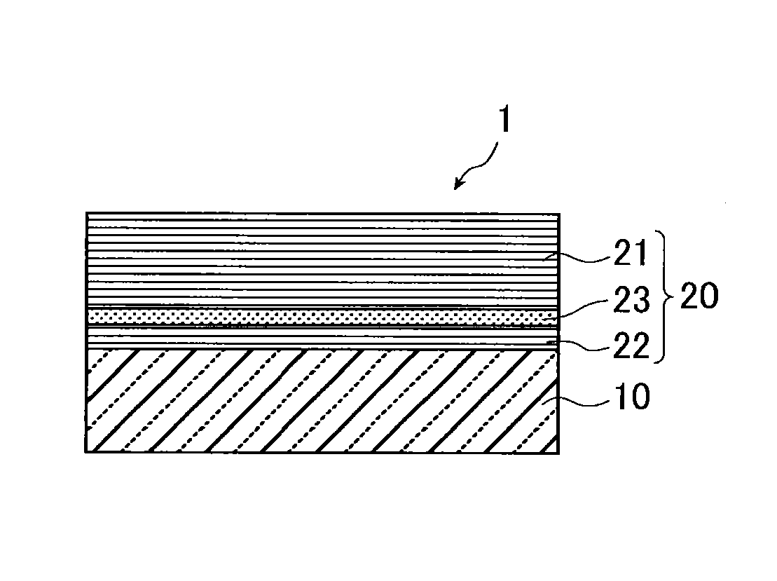
[0158]In this Example, a reflective layer-coated substrate 1 for EUVL as shown in FIG. 1 was prepared.

[0159]As a substrate 10 for film formation, a SiO2—TiO2 type glass substrate (size: 6 inches (152.4 mm) square, thickness: 6.3 mm) was used. The thermal expansion coefficient of this glass substrate was 0.05×10⁷ / ° C., the Young's modulus was 67 GPa, the Poisson ratio was 0.17, and the specific rigidity was 3.07×10⁷ m2 / s2. This glass substrate was polished to form a smooth surface having a surface roughness rms of at most 0.15 nm and a planarity of at most 100 nm on the main surface side on which a reflective layer was to be formed.

[0160]On the rear surface side of the substrate 10, a Cr film having a thickness of 100 nm was formed by a magnetron sputtering method to provide an electrically conductive coating (not shown in the drawings) having a sheet resistance of 100Ω / □.

[0161]By using the formed Cr film, the substrate 10 (size: 6 inches (152.4 mm) square, thickness: 6.3 mm) was fix...

example 2

[0193]This Example was carried out in the same manner as in Example 1 except that the second multilayer reflective film 22, the adjustment layer 23 and the first multilayer reflective film 21 were as follows.

Second Multilayer Reflective Film 22

[0194]Mo layer: 3 nm

[0195]Si layer: 4 nm

[0196]Second cycle length d2: 7 nm (0.9d1≦d2≦1.1d1 is satisfied.)

[0197]Mo layer / d2: 0.43 (from 0.25 to 0.55 is satisfied.)

[0198]Number of sets: 10 (from 3 to 31 sets is satisfied.)

[0199]Total thickness: 70 nm

Adjustment Layer 23

[0200]Mo layer: 2.4 nm

[0201]Si layer: 1.6 nm

[0202]Third cycle length d3: 4 nm (d3≦0.8d1 is satisfied.)

[0203]Mo layer / d3: 0.6 (from 0.3 to 0.7 is satisfied.)

[0204]Number of sets: 8

[0205]Total thickness L: 32 nm (as i=4, (0.3+4)d1≦L≦(0.7+4)d1 is satisfied.)

First Multilayer Reflective Film 21

[0206]Mo layer: 3 nm

[0207]Si layer: 4 nm

[0208]First cycle length d1: 7 nm (6.8 nm≦d1≦7.2 nm is satisfied.)

[0209]Mo layer / d1: 0.43 (from 0.25 to 0.55 is satisfied.)

[0210]Number of sets: 30 (from 20...

example 3

[0216]This Example was carried out in the same manner as in Example 1 except that the second multilayer reflective film 22, the adjustment layer 23 and the first multilayer reflective film 21 were as follows.

Second Multilayer Reflective Film 22

[0217]Mo layer: 3 nm

[0218]Si layer: 4 nm

[0219]Second cycle length d2: 7 nm (0.9d1≦d2≦1.1d1 is satisfied.)

[0220]Mo layer / d2: 0.43 (from 0.25 to 0.55 is satisfied.)

[0221]Number of sets: 10 (from 3 to 31 sets is satisfied.)

[0222]Total thickness: 70 nm

Adjustment Layer 23

[0223]Mo layer: 1.6 nm

[0224]Si layer: 2.4 nm

[0225]Third cycle length d3: 4 nm (d3≦0.8d1 is satisfied.)

[0226]Mo layer / d3: 0.4 (from 0.3 to 0.7 is satisfied.)

[0227]Number of sets: 1

[0228]Total thickness L: 4 nm (as i=0, (0.3+0)d1≦L≦(0.7+0)d1 is satisfied.)

[0229]First multilayer reflective film 21

[0230]Mo layer: 3 nm

[0231]Si layer: 4 nm

[0232]First cycle length d1: 7 nm (6.8 nm≦d1≦7.2 nm is satisfied.)

[0233]Mo layer / d1: 0.43 (from 0.25 to 0.55 is satisfied.)

[0234]Number of sets: 30 (fr...


PUM


Abstract

To provide a mask blank for EUVL wherein the incident angle dependence of EUV reflectivity and the film stress in a Mo/Si multilayer reflective film are improved, and a reflective layer-equipped substrate for such a mask blank. The reflective layer-equipped substrate for EUV lithography (EUVL), comprises a substrate, and a reflective layer for reflecting EUV light, formed on the substrate, wherein the reflective layer comprises a second multilayer reflective film having a Mo layer and a Si layer alternately stacked plural times on the substrate, an adjustment layer stacked on the second multilayer reflective film, and a first multilayer reflective film having a Mo layer and a Si layer alternately stacked plural times on the adjustment layer.

Description

BACKGROUND OF INVENTION[0001]1. Field of Invention[0002]The present invention relates to a reflective mask blank for EUV (Extreme Ultraviolet) lithography (hereinafter referred to also as “EUV mask blank” in this specification) to be used for e.g. production of semiconductors.[0003]Further, the present invention relates to a reflective layer-coated substrate for EUV lithography (EUVL). The reflective layer-coated substrate for EUVL is useful as a precursor for a mask blank for EUVL.[0004]2. Discussion of Background[0005]Heretofore, in the semiconductor industry, a photolithography method employing visible light or ultraviolet light has been used as a technique to transfer a fine pattern required to form an integrated circuit with a fine pattern on e.g. a silicon substrate. However, the conventional photolithography method has come close to its limit, while miniaturization of semiconductor devices is being accelerated. In the case of the photolithography method, the resolution limit ...

Claims


Application Information

Patent Timeline
IPC IPC(8): G03F1/24
CPCG03F1/24
Inventor KINOSHITA, TAKERU
Owner ASAHI GLASS CO LTD
Why Eureka
Try Eureka