

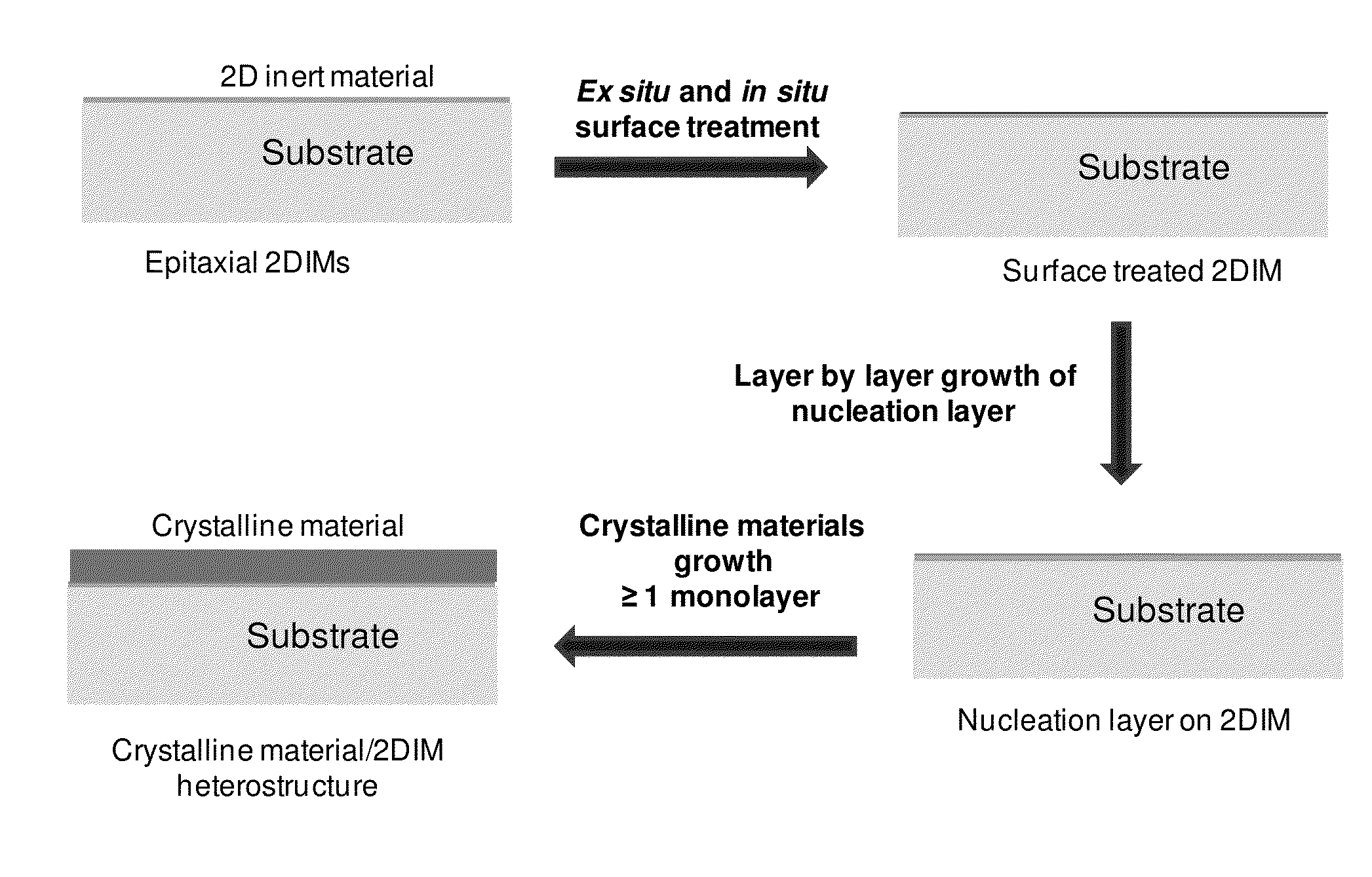
Growth of Crystalline Materials on Two-Dimensional Inert Materials
- Summary
- Abstract
- Description
- Claims
- Application Information
AI Technical Summary
Benefits of technology
Problems solved by technology
Method used
Image

Examples
example 1
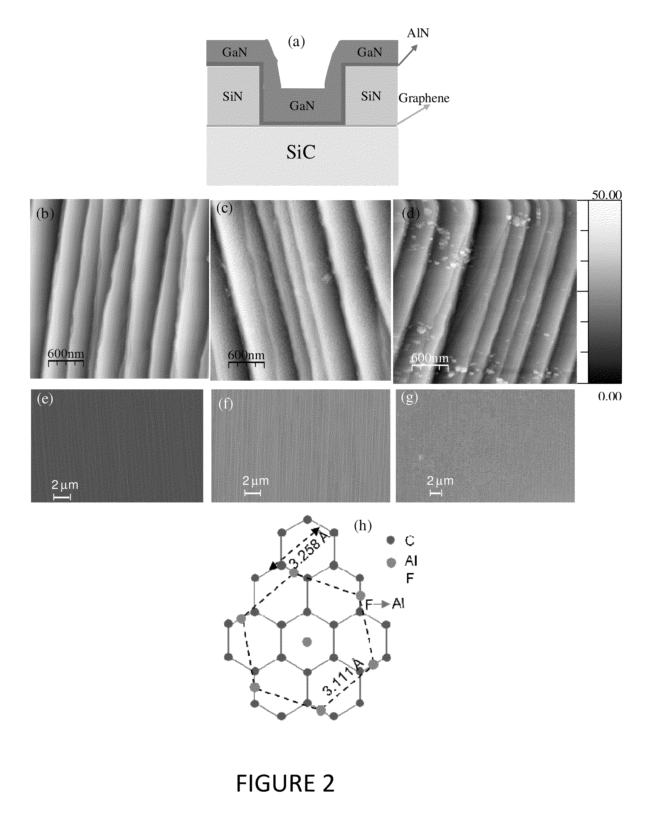
[0024]As shown in the layer structure of FIG. 2(a), crystalline materials, for example thin AlN and GaN layers, were grown on 2DIM, for example graphene.
[0025]The starting pristine graphene was about 4-5 layers thick and it follows the surface morphology of the underlying SiC, with step edges and terraces as shown in AFM and SEM images in FIGS. 2(b) and (e), respectively. At optimized ALE growth conditions, AlN is deposited uniformly on graphene; AFM and SEM images of 1.2 nm AlN on XeF2 functionalized graphene in FIGS. 2(c) and (f) show uniform nucleation.
[0026]FIGS. 2(d) and (g) show AFM and SEM images of epitaxial GaN on graphene using a 11 nm ALE AlN as a nucleation layer. In FIG. 2(h) we propose that the AlN lattice alignment along the m-plane to fluorinated graphene replacing a semi-ionically bound F atom by an Al atom without damaging the graphene lattice. The lattice mismatch between graphene and AlN is 4.5%, which is significantly smaller than the 13% between AlN and sapphir...
example 2
[0048]EG was grown on 4° 4H—SiC (16×16 mm2) samples using the Si sublimation method. The synthesized EG layers were characterized using atomic force microscopy (AFM), LEO supra 55 scanning electron microscopy (SEM), Thermo Scientific K-Alpha x-ray photo electron spectroscopy (XPS), and room temperature Raman and photoluminescence measurements.
[0049]The Raman characterization was performed using an InVia Raman microscope (Renishaw) equipped with a 50× objective lens, a 514.5 nm diode laser excitation, at a set power of 20 mW at the source with a spot size of 5 μm.
[0050]Following initial characterization, the EG / SiC was patterned with SiNx deposited by plasma-enhanced chemical vapor deposition using standard photolithography and liftoff techniques. The patterned EG was functionalized using six, 30-second pulses of a XeF2 plasma to form about 6-7% of “semi-ionic” C—F bonds.
[0051]The selectively functionalized graphene was then inserted into a Fiji ALE reactor (Cambridge NanoTech, Inc.)...
PUM
 Abstract
Description
Claims
Application Information