Programmable logic device

a logic device and programmable technology, applied in logic circuit coupling/interface arrangement, pulse technique, instruments, etc., can solve the problems of complex control logic and difficulty in fine-grained multi-context pld to precisely control power

Active Publication Date: 2014-12-18
SEMICON ENERGY LAB CO LTD
View PDF6 Cites 39 Cited by
  • Summary
  • Abstract
  • Description
  • Claims
  • Application Information

AI Technical Summary

Benefits of technology

[0028]According to one embodiment of the present invention, it is possible to provide a programmable logic device with a novel structure, i.e., a fine-grained multi-context PLD that can retain data of a register in a programmable logic element. According to one embodiment of the present invention, it is possible to provide a programmable logic device with a novel structure, i.e., a fine-grained multi-context PLD that can control power precisely by power gating in each programmable logic element without the use of a complex control circuit.

Problems solved by technology

In the case where operation of stopping supply of power to a programmable logic element that is unnecessary for processing, i.e., ‘power gating (PG)’ is employed to reduce power consumption, it is difficult for a coarse-grained multi-context PLD to control power precisely because a control unit is large.
However, a control logic is complex when the fine-grained multi-context PLD controls power in each programmable logic element.
In addition, a fine-grained multi-context PLD including an SRAM loses data stored in a register in a programmable logic element by power gating.

Method used


Image

  • Programmable logic device
  • Programmable logic device
  • Programmable logic device

Examples


embodiment 1

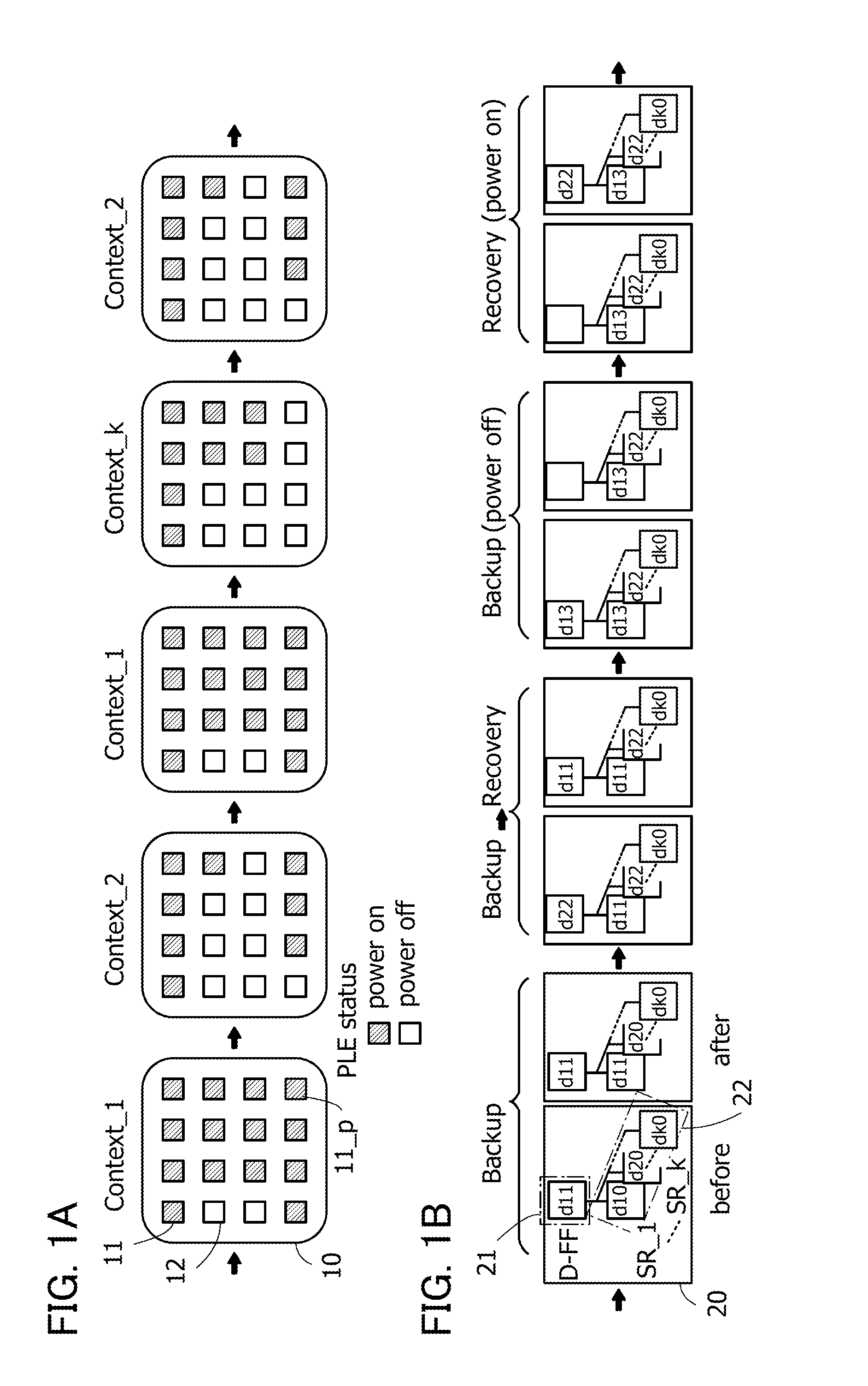
[0064]In this embodiment, PLD structures are described. FIGS. 1A and 1B are schematic diagrams illustrating PLD structures and PLD function effects.

[0065]A PLD 10 in FIG. 1A includes a plurality of programmable logic elements. FIG. 1A illustrates programmable logic elements by blocks. The programmable logic element can control power supply in each unit block. In FIG. 1A, a state in which power is supplied to programmable logic elements 11 represented by oblique hatching, i.e., a power-on state, and a state in which supply of power to programmable logic elements 12 is stopped, i.e., a power-off state are illustrated.

[0066]For example, FIG. 1A illustrates a state in which by switching first to k-th context signals (k is a natural number of 2 or more), a circuit structure is changed from a circuit structure using a first context (context—1) to a circuit structure using a second context (context—2), the circuit structure using the first context (context—1), a circuit structure using a k...

embodiment 2

[0095]In this embodiment, a circuit structure example of a PLD, a circuit structure example of a programmable logic element, and a circuit structure example of each circuit included in the programmable logic element are described.

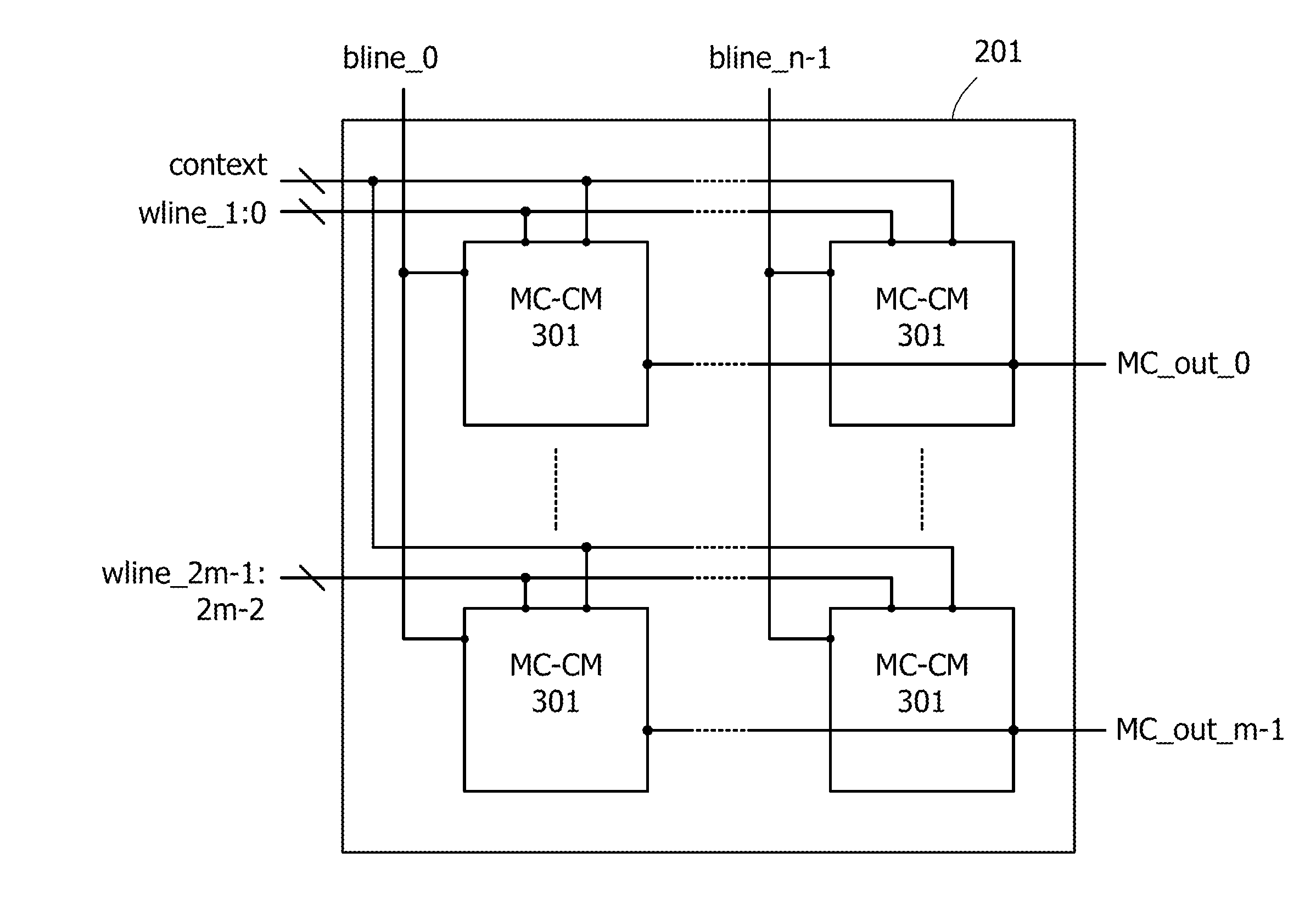
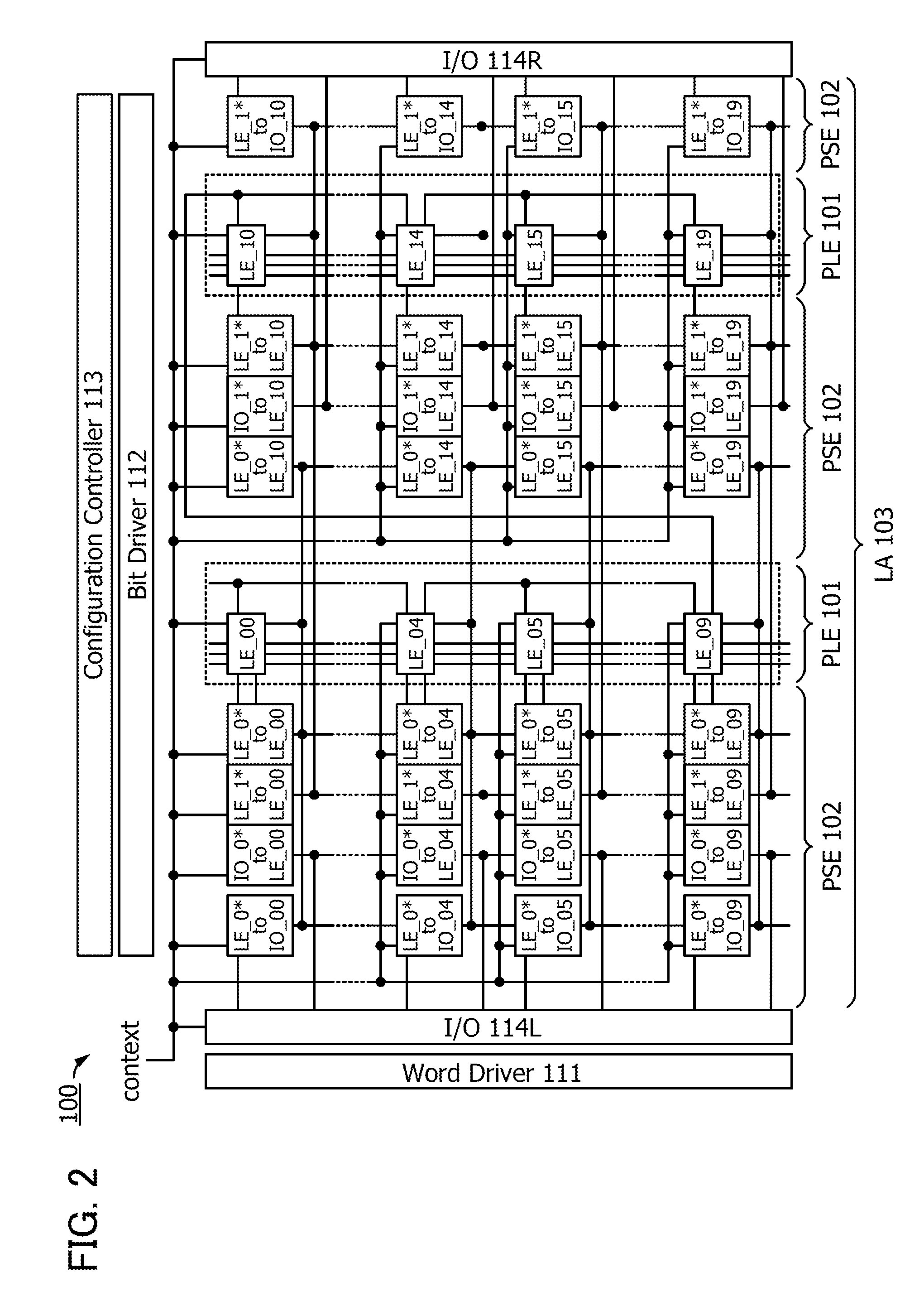
[0096]A structure example of a PLD is described. Part of the structure of a PLD 100 is illustrated in FIG. 2.

[0097]As the structure of the PLD 100, FIG. 2 illustrates a block diagram in which a logic array 103 (abbreviated to LA) including programmable logic elements 101 (abbreviated to PLE) and programmable switch elements 102 (abbreviated to PSE), a word line driver circuit 111 (Word Driver), a bit line driver circuit 112 (Bit Driver), a configuration control circuit 113 (Configuration Controller), an input / output terminal portion 114L (I / O), and an input / output terminal portion 114R (I / O) are provided.

[0098]FIG. 2 illustrates an example in which the programmable logic elements 101 and the programmable switch elements 102 are arranged in a column directio...

embodiment 3

[0184]In this embodiment, an oxide semiconductor layer that can be used as the semiconductor layer of the transistor with low off-state current described in the above embodiment is described.

[0185]An oxide semiconductor used for a channel formation region in the semiconductor layer of the transistor preferably contains at least indium (In) or zinc (Zn). In particular, In and Zn are preferably contained. A stabilizer for strongly bonding oxygen is preferably contained in addition to In and Zn. As a stabilizer, at least one of gallium (Ga), tin (Sn), zirconium (Zr), hafnium (Hf), and aluminum (Al) may be contained.

[0186]As another stabilizer, one or more kinds of lanthanoid such as lanthanum (La), cerium (Ce), praseodymium (Pr), neodymium (Nd), samarium (Sm), europium (Eu), gadolinium (Gd), terbium (Tb), dysprosium (Dy), holmium (Ho), erbium (Er), thulium (Tm), ytterbium (Yb), and lutetium (Lu) may be contained.

[0187]As the oxide semiconductor used for the semiconductor layer of the t...


PUM


Abstract

Data of a register in a programmable logic element is retained. A volatile storage circuit and a nonvolatile storage circuit are provided in a register of a programmable logic element whose function can be changed in response to a plurality of context signals. The nonvolatile storage circuit includes nonvolatile storage portions for storing data in the register. The number of nonvolatile storage portions corresponds to the number of context signals. With such a structure, the function can be changed each time context signals are switched and data in the register that is changed when the function is changed can be backed up to the nonvolatile storage portion in each function. In addition, the function can be changed each time context signals are switched and the data in the register that is backed up when the function is changed can be recovered to the volatile storage circuit.

Description

BACKGROUND OF THE INVENTION[0001]1. Field of the Invention[0002]The present invention relates to programmable logic devices. Furthermore, one embodiment of the present invention relates to semiconductor devices and the like including the programmable logic devices.[0003]2. Description of the Related Art[0004]A programmable logic device (PLD) includes a plurality of programmable logic elements and a plurality of programmable switch elements. The circuit structure and function of the PLD can be changed by changing the function of each programmable logic element or connection between programmable logic elements that is established with programmable switch elements by programming performed by a user after manufacture.[0005]A multi-context PLD that stores a set of configuration data corresponding to a plurality of circuit structures and changes its circuit structure by selecting the set of configuration data to be used has been actively studied (for example, see Non-Patent Document 1). I...

Claims


Application Information

Patent Timeline
Patent Type & Authority Applications(United States)
IPC IPC(8): H03K19/00H03K19/0185
CPCH03K19/018585H03K19/0013
Inventor AOKI, TAKESHIKUROKAWA, YOSHIYUKIKOZUMA, MUNEHIRONAKAGAWA, TAKASHI
Owner SEMICON ENERGY LAB CO LTD
Why Eureka
Try Eureka