Method for Production of Optical Waveguides and Coupling and Devices Made from the Same

a technology of optical waveguides and couplings, applied in the field of production of highlyconfined optical nanowaveguides, can solve the problems of conventional etching methods, large optical waveguides which are not suitable for many novel optical circuits, and optical energy to leak or radiate out, and achieve low loss optical waveguides, high-refractive index contrast, and high-refractive index contrast

Active Publication Date: 2015-01-01
PARTOW TECH LLC
View PDF7 Cites 24 Cited by
  • Summary
  • Abstract
  • Description
  • Claims
  • Application Information

AI Technical Summary

Benefits of technology

[0018]Summary and Abstract summarize some aspects of the present invention. Simplifications or omissions may have been made to avoid obscuring the purpose of the Summary or the Abstract. These simplifications or omissions are not intended to limit the scope of the present invention.
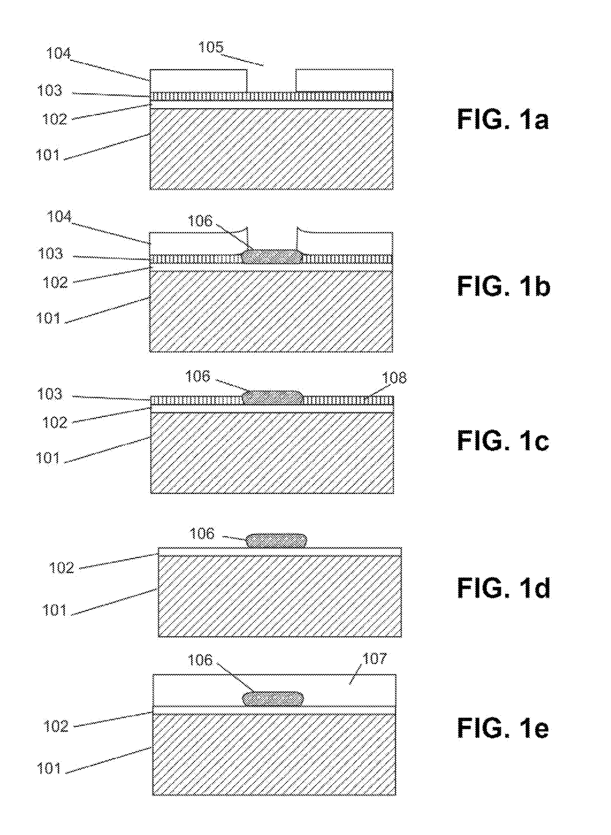
[0019]In one embodiment of the invention, a method for producing a high-refractive index contrast and low loss optical waveguide is disclosed. This method comprises the steps of: depositing a lower cladding material layer with a first low refractive index on a silicon base substrate; depositing or growing a refractory metal layer on top of the lower cladding material layer with the first low refractive index; forming a trench in a top diffusion barrier layer deposited on the refractory metal layer, wherein the trench has an open surface for the refractory metal layer; oxidizing the open surface of the trench to high-temperature ambient oxygen, wherein the open surface subsequently forms an oxidized refractory metal region, and wherein other parts of the refractory metal layer still covered under the top diffusion layer remain unchanged as a non-oxidized refractory metal region; removing the top diffusion barrier layer using one or more chemical etching agents; removing the non-oxidized refractory metal region by using a dry-etching tool with high-etch selectivity to preserve the oxidized refractory metal region; and depositing a top cladding layer made of a second low refractive index material to encapsulate the oxidized refractory metal region on top of the lower cladding material layer.
[0020]In another embodiment of the invention, a method for producing a high-refractive index contrast and low loss optical waveguide is disclosed. This method comprises the steps of: depositing a lower cladding material layer with a first low refractive index on a silicon base substrate; depositing or growing a refractory metal layer on top of the lower cladding material layer with the first low refractive index; forming an etch mask layer deposited on the refractory metal layer; selectively etching the refractory metal layer in a dry etching tool with high selectivity to the etch mask layer; oxidizing the refractory metal layer at high-temperature ambient oxygen, wherein the refractory metal layer subsequently forms an oxidized refractory metal region; and depositing a top cladding layer made of a second low refractive index material to encapsulate the oxidized refractory metal region on top of the lower cladding material layer.
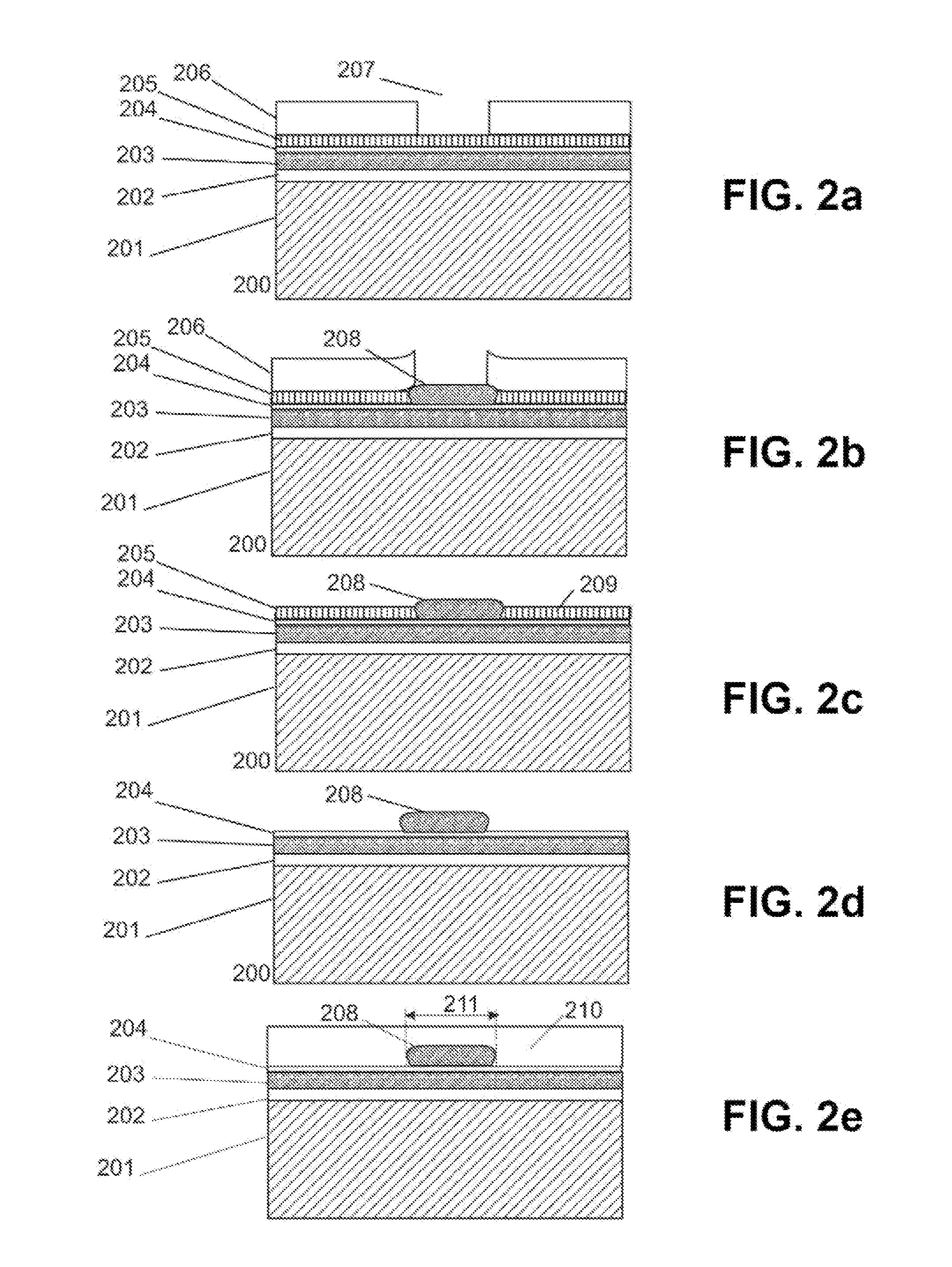
[0021]In another embodiment of the invention, a method for producing a high-refractive index contrast and low loss optical waveguide is disclosed. This method comprises the steps of: depositing or growing a low refractive index cladding layer on top of a silicon base substrate; depositing or transferring a high refractive index optical material layer on top of the low refractive index cladding layer to form a slab core region; depositing a thin optically-transparent layer on top of the slab core region; depositing or growing a refractory metal layer on top of the optically-transparent layer; forming a trench in a top diffusion barrier layer on the refractory metal layer, wherein the trench has an open surface for the refractory metal layer; oxidizing the open surface by exposing the open surface of the refractory metal layer to high-temperature ambient oxygen, wherein the open surface of the refractory metal layer subsequently forms an oxidized refractory metal region, and wherein other parts of the refractory metal layer still covered under the top diffusion layer remain unchanged as a non-oxidized refractory metal region; removing the top diffusion barrier layer using one or more chemical etching agents; removing the non-oxidized refractory metal region by using a dry-etching tool with high-etch selectivity to preserve the oxidized refractory metal region; and depositing a top cladding layer made of a second low refractive index material to encapsulate the oxidized refractory metal region.
[0022]In another embodiment of the invention, a method for producing a high-refractive index contrast and low loss optical waveguide is disclosed. This method comprises the steps of: depositing or growing a low refractive index cladding layer on top of a silicon base substrate; depositing or transferring a high refractive index optical material layer on top of the low refractive index cladding layer to form a slab core region; depositing a thin optically-transparent layer on top of the slab core region; depositing or growing a refractory metal layer on top of the thin optically transparent layer; forming an etch mask layer deposited on the refractory metal layer; selectively etching the refractory metal layer in a dry etching tool with high selectivity to the etch mask layer; oxidizing the refractory metal layer at high-temperature ambient oxygen, wherein the refractory metal layer subsequently forms an oxidized refractory metal region; and depositing a top cladding layer made of a second low refractive index material to encapsulate the oxidized refractory metal region on top of the lower cladding material layer.

Problems solved by technology

Furthermore, a low-confinement optical waveguide is typically curved into a radius typically larger than 0.5 mm, because a radius smaller than approximately 0.5 mm may cause the optical energy to leak or radiate out.
However, these conventional methods create low-confinement optical waveguides, resulting in large optical waveguides which are not suitable for many novel optical circuits.
However, because the sidewall roughness scattering losses are very important in highly-confined optical waveguides, conventional etching methods present significant challenges.
For example, an optical waveguide produced by using lithography and etching typically suffers from nano-meter scale sidewall roughness, which scatters the light out of the core layer of the highly-confined waveguides.
Furthermore, the etching of ferroelectric materials such as lithium niobate and lithium tantalate is very difficult.
For example, in many situations, it is not possible to achieve straight sidewalls required for highly-confined waveguides when the etching of certain ferroelectric materials are attempted.
However, silicon is not transparent in most of optical spectrum and has a very high refractive index, which complicates the fabrication of many optical circuits.
This method for coupling the light to high-index contrast waveguides requires a plurality of small optical lenses and individual alignment for each lens, which is time consuming and expensive to manufacture.
The GRIN lens method disclosed in these publications requires a precise control of refractive index profile, and it is generally difficult to manufacture an exact refractive index profile with a high level of precision.
Unfortunately, the fabrication of grating coupler is difficult because of very small feature size manufacturing requirements.
In addition, there are light scattering-related losses associated with the grating coupler.
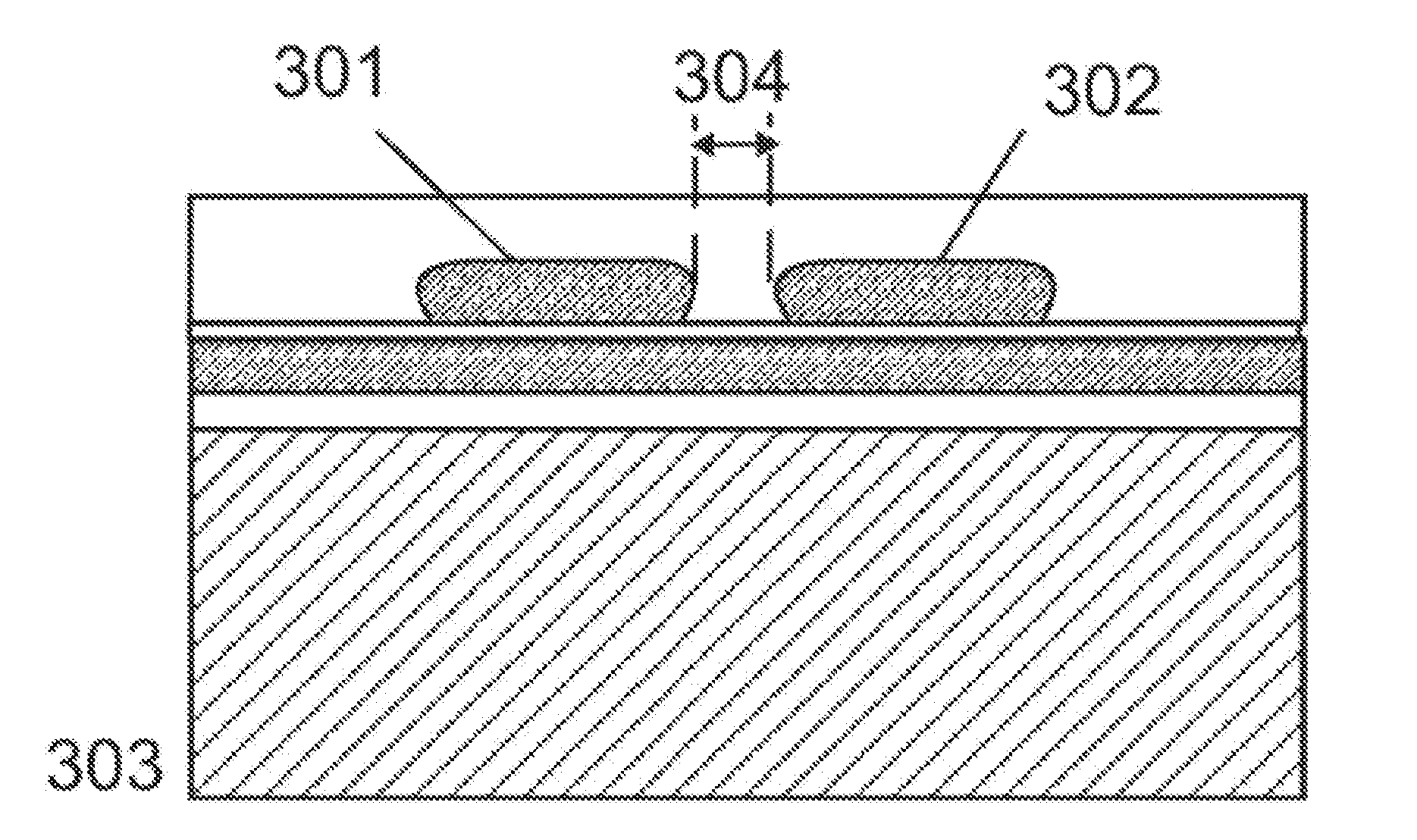
Because the mode size of a nano waveguide is very small compared to the mode size of an optical fiber (i.e. typically less than 1 micron for a nano waveguide, compared to 10 microns for an optical fiber), the coupling efficiency from an optical fiber to a high-index contrast waveguide is very poor.

Method used


Image

  • Method for Production of Optical Waveguides and Coupling and Devices Made from the Same
  • Method for Production of Optical Waveguides and Coupling and Devices Made from the Same
  • Method for Production of Optical Waveguides and Coupling and Devices Made from the Same

Examples


Embodiment Construction

[0039]Specific embodiments of the invention will now be described in detail with reference to the accompanying figures. Like elements in the various figures are denoted by like reference numerals for consistency.

[0040]In the following detailed description of embodiments of the invention, numerous specific details are set forth in order to provide a more thorough understanding of the invention. However, it will be apparent to one of ordinary skill in the art that the invention may be practiced without these specific details. In other instances, well-known features have not been described in detail to avoid unnecessarily complicating the description.

[0041]The detailed description is presented largely in terms of procedures, logic blocks, processing, and / or other symbolic representations that directly or indirectly resemble a novel high-refractive index contrast waveguide, a method of manufacturing a high-refractive index contrast waveguide, and / or a method of low loss and efficient op...


PUM

PropertyMeasurementUnit
thicknessaaaaaaaaaa
thicknessaaaaaaaaaa
refractive indexaaaaaaaaaa

Abstract

Novel processing methods for production of high-refractive index contrast and low loss optical waveguides are disclosed. In one embodiment, a “channel” waveguide is produced by first depositing a lower cladding material layer with a low refractive index on a base substrate and a refractory metal layer. Then, an etch mask layer is deposited on the refractory layer, followed by selective etching of the refractory metal layer with a dry-etch tool with high selectivity to the etch mask layer. Then, the refractory metal layer is oxidized to form an oxidized refractory metal region, and a top cladding layer made of a second low refractive index material to encapsulate the oxidized refractory metal region. In another embodiment, a “ridge” waveguide is produced by using similar process steps with an added step of depositing a high-refractive-index material layer and an optional optically-transparent layer.

Description

FIELD OF THE INVENTION[0001]The present invention generally relates to a method for production of highly-confined optical nano-waveguides and a method for coupling optical energy from an optical fiber to the highly-confined optical nano-waveguide. Furthermore, the present invention also relates to a method for creating high-confinement optical nano-waveguides in optical materials such as lithium niobate, lithium tantalate, tantalum oxide, and niobium oxide. In addition, the present invention also relates to a method for fabricating optical waveguides that can simultaneously achieve high confinement, low loss, high precision, and narrow nano-gap between adjacent waveguides for coupled waveguide devices. The present invention also relates to a novel device and fabrication method for coupling optical energy from an optical fiber to an optical nano-waveguide.BACKGROUND OF THE INVENTION[0002]In numerous electronic communication applications, optical waveguides are used in various optical...

Claims


Application Information

Patent Timeline
Patent Type & Authority Applications(United States)
IPC IPC(8): H01J37/32G02B6/10
CPCH01J37/32366G02B6/10B82Y20/00G02B6/107G02B6/12033G02B6/1223G02B6/136G02B2006/1204G02B2006/12045G02B2006/12054G02B2006/12057G02B2006/12097G02F1/035G02F1/225G02F1/3558G02F2201/30G02F2202/20B82Y40/00G02B6/02295G02B6/03677C23C14/34G02B2207/101
Inventor RABIEI, PAYAM
Owner PARTOW TECH LLC
Why Eureka
Try Eureka