Method for producing printed-wiring board

a printing and wiring board technology, applied in the direction of liquid/solution decomposition chemical coating, instruments, photomechanical equipment, etc., can solve the problems of inability to form a pattern, difficult to form a fine pattern with a wiring width of less than 10 m, and inability to obtain sufficient adhesion, etc., to achieve low etching amount, low roughness degree, and fine unevenness roughening

Active Publication Date: 2015-02-05
MITSUBISHI GAS CHEM CO INC
View PDF7 Cites 12 Cited by
  • Summary
  • Abstract
  • Description
  • Claims
  • Application Information

AI Technical Summary

Benefits of technology

[0027]According to the method for producing a printed-wiring board of the present invention, in the production of a printed-wiring board by means of a semi-additive process that was conventionally difficult, by subjecting a chemical copper plating or a copper film formed by the sputtering method (sputtered copper), which is a seed layer, to a fine unevenness roughening with a low etching amount and a low roughness degree, it is possible to suppress reduction in the resolution due to light scattering in the exposure process, and it is also possible to improve adhesion to a dry film resist after the development and to strip the dry film resist without residue, thereby forming a micro wiring. Therefore, the method has a great deal of potential in industry.

Problems solved by technology

However, the surface of the conventional chemical copper plating that is formed on the insulation layer coarsely roughened is markedly uneven, and therefore, in the exposure process for a dry film resist, it is difficult to form a fine pattern with a wiring width of less than 10 μm because of reduction in the resolution due to light scattering.
In the case of the surface of chemical copper plating, adhesion to a dry film resist material is insufficient, and it is impossible to form a pattern.
The surface of the sputtered copper is flatter and smoother than the chemical copper plating, and it is impossible to obtain sufficient adhesion to a dry film resist material, and therefore, it is difficult to form a pattern.
For this reason, stripping is insufficient.
Further, dry film resist materials for micro wiring formation have been improved to be a low-swelling type having a high resolution, and therefore, such resists cannot be stripped with conventional stripping liquids.

Method used


Image

  • Method for producing printed-wiring board
  • Method for producing printed-wiring board
  • Method for producing printed-wiring board

Examples


example 1

[0062]

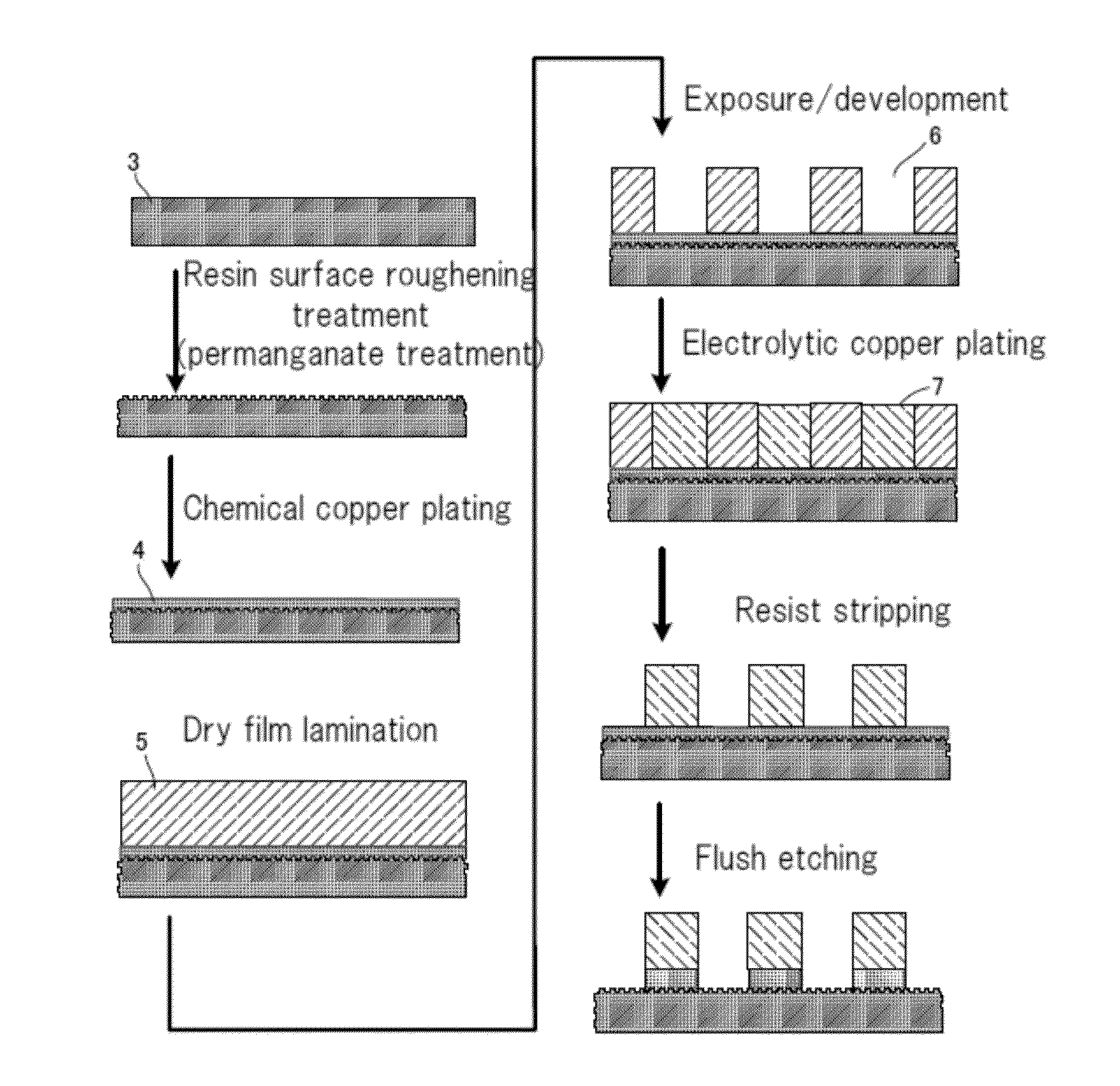
[0063]A substrate of chemical copper plating (size: 15 cm×15 cm, thickness of plating: 0.5 μm) was subjected to a spray treatment at a liquid temperature of 30° C. and a spray pressure of 0.1 MPa for 30 seconds using an etching solution prepared with 0.3% by mass of hydrogen peroxide, 1.5% by mass of sulfuric acid, 0.1% by mass of 5-methyltetrazole, 1 ppm of chloride ion and the remaining amount of water. As a result, the amount of dissolution of copper was 0.2 μm. The specific amount of dissolution of copper was calculated from the difference in mass of the substrate before and after the roughening treatment.

[0064]Next, with respect to the surface of chemical copper plating after etching, the surface area in an area of 5 μm×5 μm was measured using a scanning tunneling microscope (30,000x). As a result, the surface area of the chemical copper plating was 38 [μm2]. The specific surface area was 38 [μm2] / 25 [μm2]=1.52. Further, the copper surface roughness (Ra) was 0.17 μm. An e...

example 2

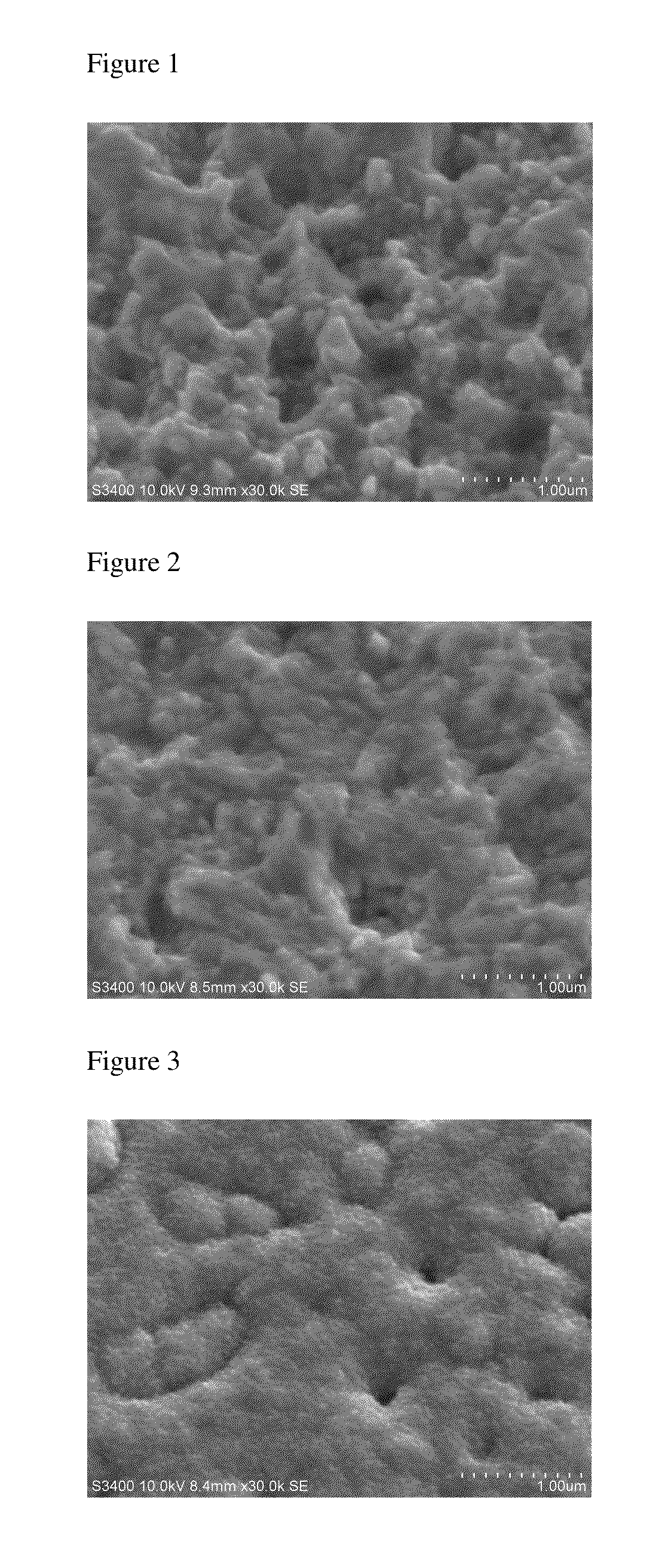
[0067] and were carried out in manners similar to those in Example 1, except that an etching solution was prepared with 0.5% by mass of hydrogen peroxide, 2.5% by mass of sulfuric acid, 0.05% by mass of 5-aminotetrazole, 0.05% by mass of 1,5-dimethyltetrazole, 1 ppm of chloride ion and the remaining amount of water. The surface area of the chemical copper plating was 40 [μm2]. The specific surface area was 1.60. The copper surface roughness (Ra) was 0.20 μm. The evaluation result regarding the adhesion of the dry film is shown in Table 1, and the evaluation result regarding the dry film stripping property is shown in Table 2.

example 3

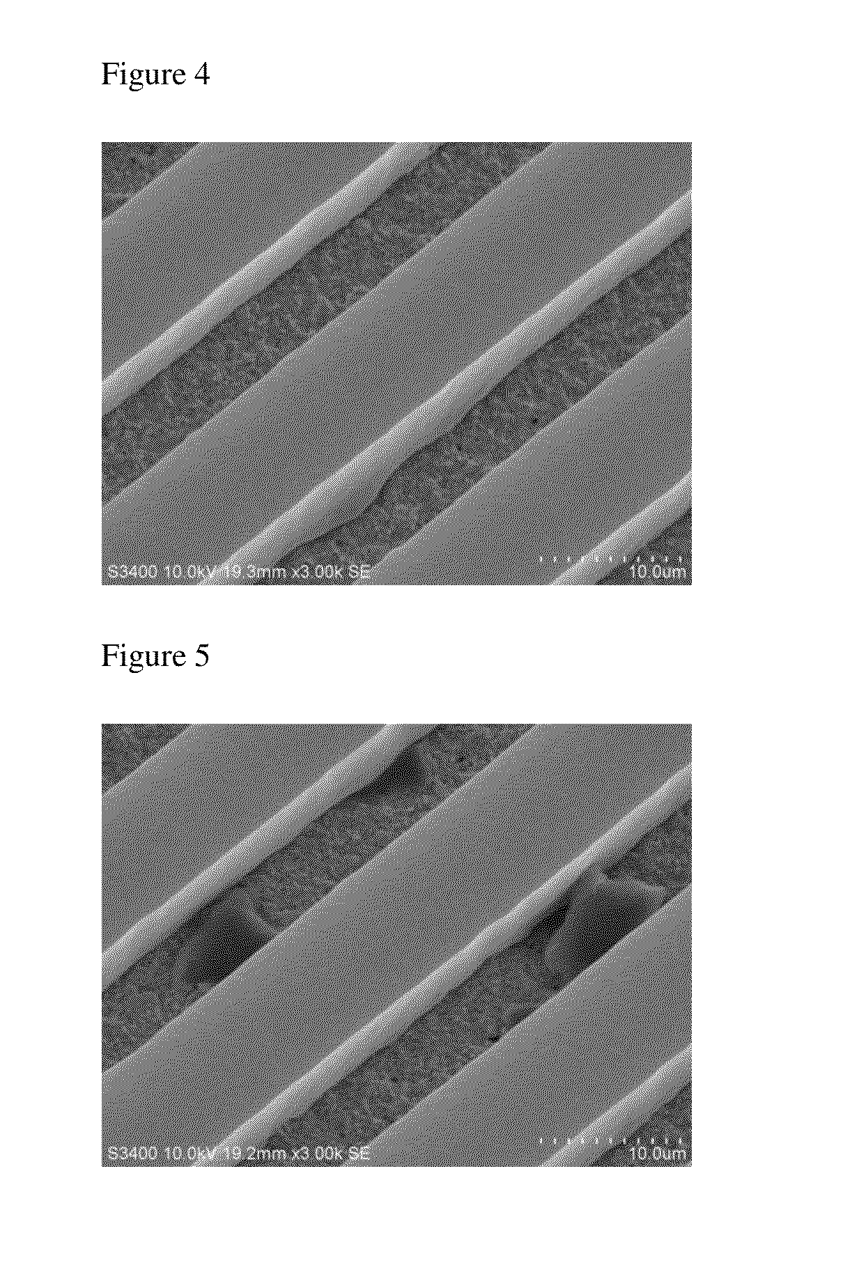
[0068] and were carried out in manners similar to those in Example 1, except that an etching solution was prepared with 0.4% by mass of hydrogen peroxide, 2% by mass of sulfuric acid, 0.05% by mass of 1H-tetrazole, 0.03% by mass of 5-mercapto-1-methyltetrazole, 1 ppm of chloride ion and the remaining amount of water. The surface area of the chemical copper plating was 37 [μm2]. The specific surface area was 1.48. The copper surface roughness (Ra) was 0.19 μm. The evaluation result regarding the adhesion of the dry film is shown in Table 1, and the evaluation result regarding the dry film stripping property is shown in Table 2.


PUM


Abstract

The present invention provides a method for producing a printed-wiring board in a semi-additive process, comprising the steps of: providing a chemical copper plating 4 on an insulation layer 3 or forming a copper thin film on the insulation layer 3 using a sputtering method; subjecting the obtained copper surface 4 to a roughening treatment using an etching solution containing 0.1 to 3% by mass of hydrogen peroxide, 0.3 to 5% by mass of sulfuric acid, 0.1 to 3 ppm of halogen ion and 0.003 to 0.3% by mass of tetrazoles; attaching a dry film resist 5 to the copper surface 4 after the roughening treatment to perform exposure and development and providing an electrolytic copper plating 7 to an opening 6 after the exposure; and subjecting the remaining dry film resist to a stripping treatment using a resist stripping liquid containing 0.5 to 20% by mass of monoethanolamine, 0.2 to 10% by mass of quaternary ammonium hydroxide, 0.01 to 10% by mass of ethylene glycols and 0.01 to 0.5% by mass of azoles.

Description

TECHNICAL FIELD[0001]The present invention relates to a method for producing a printed-wiring board to be used for electrical devices, electronic devices, etc., and specifically relates to a method for forming a micro wiring in a semi-additive process.BACKGROUND ART[0002]Recently, with miniaturization, reduction in weight and sophistication of electronic devices, refinement and density increase of copper wiring have been strongly desired for printed-wiring boards.[0003]A semi-additive process is one of production methods for forming a micro wiring. According to this method for forming a wiring, a metal layer called a seed layer is formed on an insulation layer, a plating resist layer is formed on the surface thereof, and after that, exposure and development are performed to form a resist pattern. After that, an electrolytic copper plating is provided to an opening, the resist is stripped, and the seed layer is removed by etching to form a copper wiring.[0004]Conventionally, the surf...

Claims


Application Information

Patent Timeline
Patent Type & Authority Applications(United States)
IPC IPC(8): H05K3/06H05K1/09
CPCH05K1/09H05K3/067C23C18/1653C23C18/1689C23C18/38C23F1/18C25D5/022H05K3/108H05K3/185G03F7/422H05K3/064
Inventor TAKAHASHI, KENICHIIKEDA, KAZUHIKO
Owner MITSUBISHI GAS CHEM CO INC
Why Eureka
Try Eureka