Surface treatment method for implant
a treatment method and implant technology, applied in the field of implant surface treatment, can solve the problems of excessive corrosion, adverse reactions of surrounding tissues, aesthetic problems, etc., and achieve the effects of reducing toxicity, excellent continuity and uniformity, and effectively blocking the dissociation of free metal ions
- Summary
- Abstract
- Description
- Claims
- Application Information
AI Technical Summary
Benefits of technology
Problems solved by technology
Method used
Image
Examples
example 1
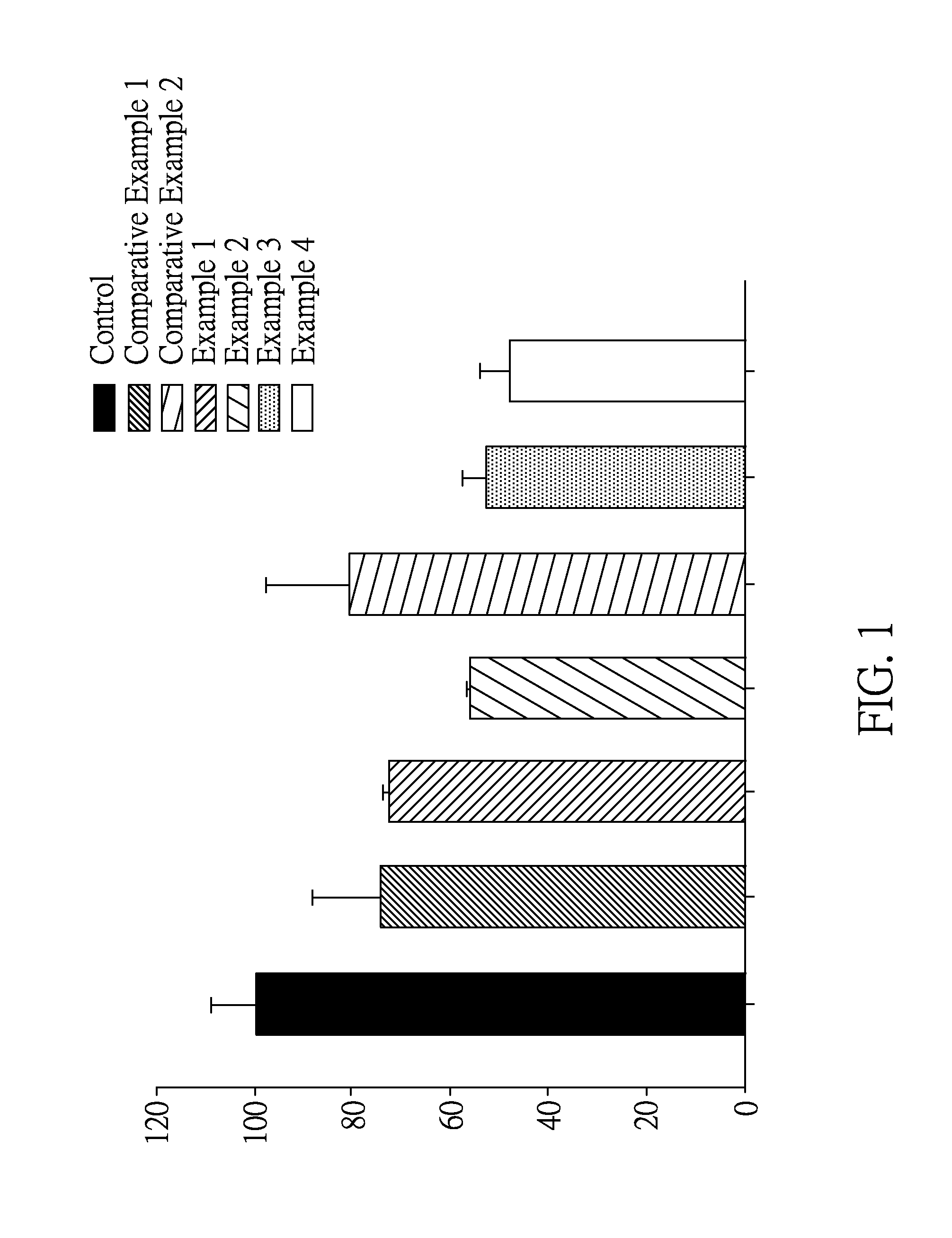
[0020]In this Example, a pure titanium (Ti) cylinder of 14 mm diameter and 2 mm height was provided as the substrate. Then, the atomic layer deposition was performed in an atomic layer deposition reactor (Savannah S100, manufactured by CambrigeNanoTech Ltd.) with tetrakis dimethylamino zirconium (TDMAZ; Zr(N(CH3)2)4) and water as the precursors at 150° C., to form a ZrO2 layer on the pure titanium substrate. The atomic layer deposition method is performed by the following steps: (1) application of pulse of zirconium dimethyl ammonium; (2) nitrogen purging; (3) application of pulse of water; and (4) nitrogen purging, which were repeated for more than 200 times, to provide ZrO2 with a thickness of 20 nm. Thereby, a ZrO2 ceramic layer having a thickness of 20 nm was formed on the pure titanium substrate.
example 2
[0021]In Example 2 the same method as in Example 1 was performed to form the ZrO2 layer on the pure titanium substrate, except that the atomic layer deposition cycle was repeated for more than 1000 times to provide ZrO2 with a thickness of 100 nm. Thereby, a ZrO2 ceramic layer having a thickness of 100 nm was formed on the pure titanium substrate.
example 3
[0022]In this Example, a titanium alloy (Ti6Al4V) cylinder of 14 mm in diameter and 2 mm in height was provided as the substrate. Then, the ZrO2 layer was formed on the Ti6Al4V substrate by the atomic layer deposition as in Example 1, except that the atomic layer deposition method was repeated for more than 200 times to provide ZrO2 with a thickness of 20 nm. Thereby, a ZrO2 ceramic layer having a thickness of 20 nm was formed on the Ti6Al4V substrate.
PUM
| Property | Measurement | Unit |
|---|---|---|
| thickness | aaaaa | aaaaa |
| root mean square roughness | aaaaa | aaaaa |
| thickness | aaaaa | aaaaa |
Abstract
Description
Claims
Application Information


