

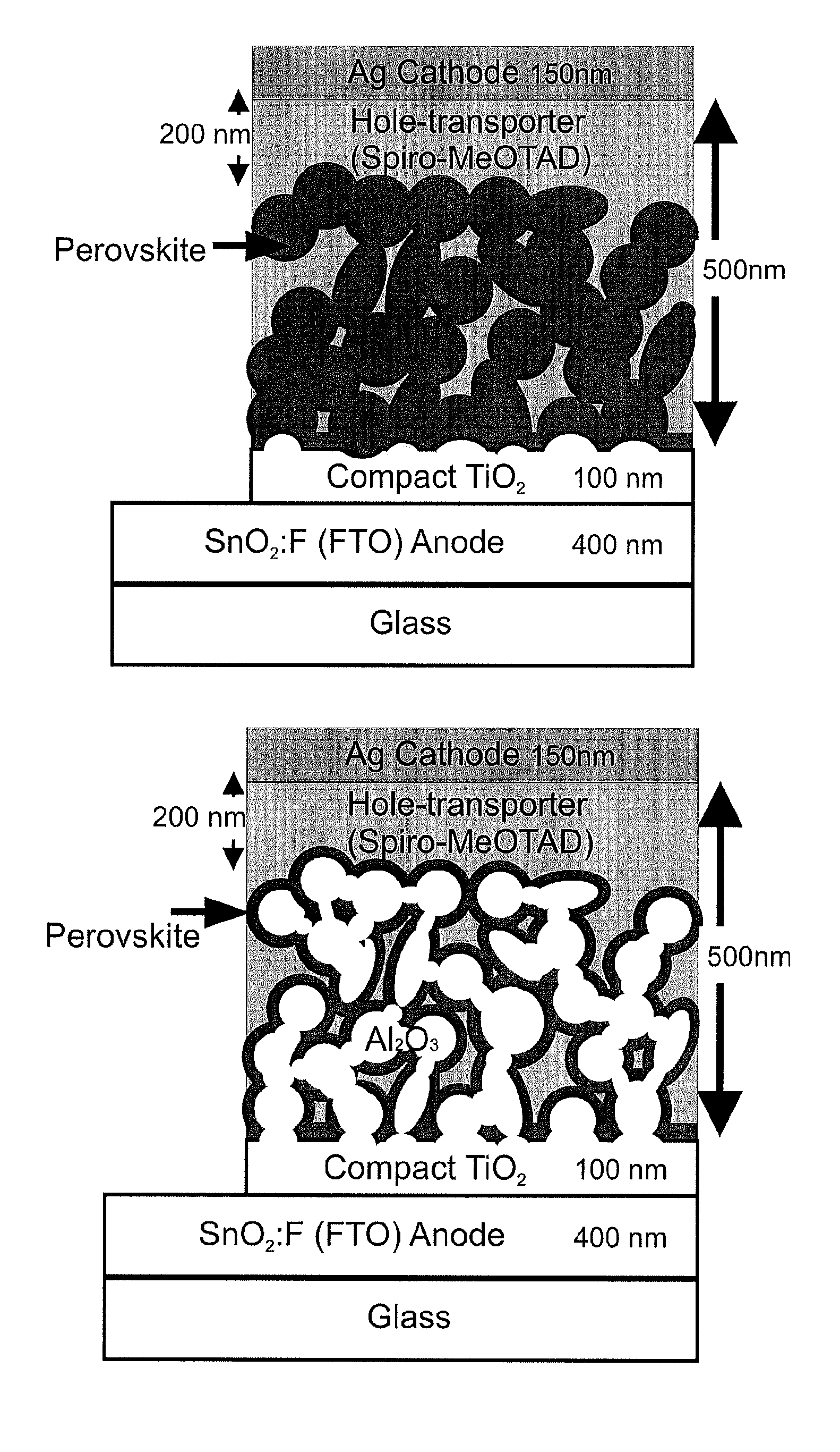
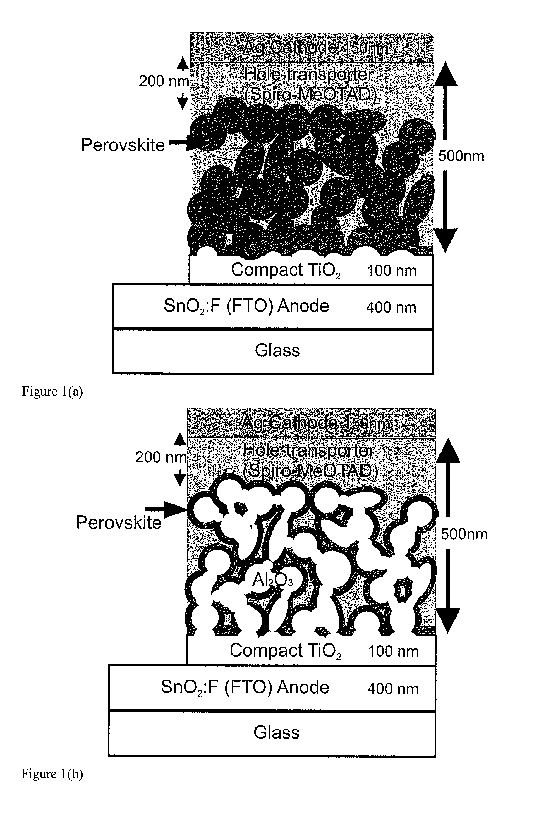
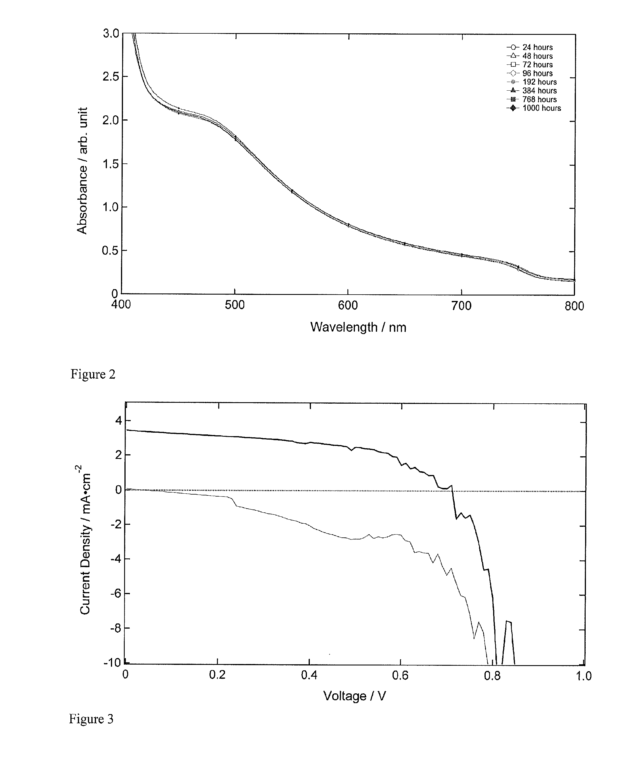
Optoelectronic device comprising perovskites
- Summary
- Abstract
- Description
- Claims
- Application Information
AI Technical Summary
Benefits of technology
Problems solved by technology
Method used
Image

Examples
examples
Experimental Description:
1. Synthesis of Organometal Halide Perovskites:
1.1. Preparation of Methylammonium Iodide Precursor
[0356]Methylamine (CH3NH2) solution 33 wt. % in absolute ethanol (Sigma-Aldrich) was reacted with hydriodic acid 57 wt. % in water (Sigma-Aldrich) at 1:1 molar ratio under nitrogen atmosphere in anhydrous ethanol 200 proof (Sigma-Aldrich). Typical quantities were 24 ml methylamine, 10 ml hydroiodic acid and 100 ml ethanol. Crystallisation of methylammonium iodide (CHNH3I) was achieved using a rotary evaporator a white coloured precipitate was formed indicating successful crystallisation.
[0357]The methylamine can be substituted for other amines, such as ethylamine, n-butylamine, tert-butylamine, octylamine etc. in order to alter the subsequent perovskite properties. In addition, the hydriodic acid can be substituted with other acids to form different perovskites, such as hydrochloric acid.
1.2. Preparation of Methylammonium Iodide Lead (II) Chloride (CH3NH3PbCl2I)...
PUM
 Abstract
Description
Claims
Application Information