
Resist underlayer film forming composition that contains novolac resin having polynuclear phenol

Active Publication Date: 2015-07-02
NISSAN CHEM IND LTD
View PDF13 Cites 11 Cited by
  • Summary
  • Abstract
  • Description
  • Claims
  • Application Information

AI Technical Summary

Benefits of technology

The present invention relates to a resist underlayer film-forming composition that provides an excellent resist underlayer film with high dry-etching resistance. The composition can be used in a process to fabricate a semiconductor substrate with a resist underlayer film as a mask. The resist underlayer film exhibits sufficient etching resistance for the fabricated substrate and can be used as a planarizing film, resist underlayer film, antifouling film, or a film having dry etching selectivity. The composition is a coating-type composition that has high heat resistance and is soluble in resist solvent. The resist underlayer film-forming composition is easy to apply and has excellent planarizing properties, embedding ability, and adhesion to substrate surfaces. The process for fabricating a semiconductor substrate using the composition includes forming a resist underlayer film on a substrate, forming a hard mask, forming a resist film, and forming a resist pattern. The resist underlayer film is made of a novolac resin that exhibits high heat resistance and does not undergo thermal degradation upon deposition of deposits.

Problems solved by technology

This trend has been accompanied by significant issues of influences due to standing waves and diffuse reflection of the active rays by irradiation from the substrate.
As a finer resist pattern is further pursued, an issue of resolution and an issue in which the resist pattern formed collapses after development may occur, and thus thinner resists are required to solve these issues.
However, in producing such thinner resists, it is difficult to achieve sufficient resist pattern film thickness for fabrication of a substrate, and thus a process has become necessary in which the function of a mask during the substrate fabrication is imparted not only to the resist pattern, but also to a resist underlayer film that is formed between the resist and a semiconductor substrate to be fabricated.
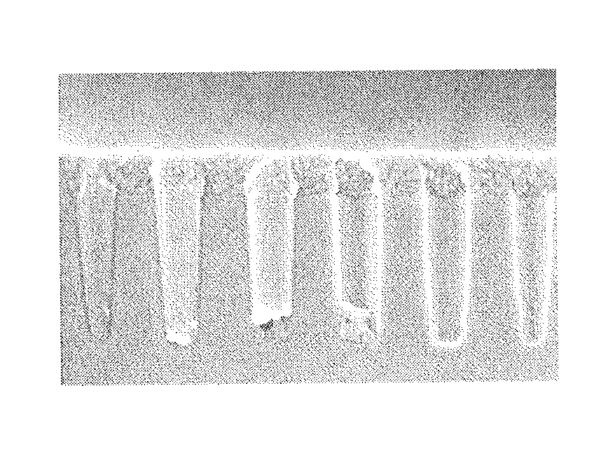
As the resist pattern becomes finer, irregular bending of the pattern called “wiggling” may occur in the resist underlayer films as etching masks during a dry-etching process, thereby hindering desired pattern formation during the semiconductor substrate fabrication.

Method used


Image

  • Resist underlayer film forming composition that contains novolac resin having polynuclear phenol
  • Resist underlayer film forming composition that contains novolac resin having polynuclear phenol
  • Resist underlayer film forming composition that contains novolac resin having polynuclear phenol

Examples


synthesis example 1

[0107]20.79 g of propylene glycol monomethyl ether was added to 8.65 g of 1,1,2,2-tetrakis(4-hydroxyphenyl)ethane (product name: TEP-DF, manufactured by Asahi Organic Chemicals Industry Co., Ltd.), 5.00 g of 1-pyrenecarboxyaldehyde (manufactured by Maruzen Chemical Industries, Ltd.), and 0.21 g of methanesulfonic acid, and this mixture was stirred under reflux for 23 hours in nitrogen atmosphere. After the reaction was completed, this solution was diluted with 35 g of tetrahydrofuran. This diluted solution was subjected to reprecipitation in a mixed solvent of methanol / water (50% by mass / 50% by mass). The obtained precipitate was filtered, and the residue was washed and then dried under reduced pressure at 60° C., whereby 9.4 g of a novolac resin was obtained (including the polymer of Formula (8-1)). The weight-average molecular weight measured in terms of standard polystyrene by GPC was 3,600.

synthesis example 2

[0108]20.02 g of propylene glycol monomethyl ether was added to 6.06 g of 1,1,2,2-tetrakis(4-hydroxyphenyl)ethane (product name: TEP-DF, manufactured by Asahi Organic Chemicals Industry Co., Ltd.), 7.00 g of 1-pyrenecarboxyaldehyde (manufactured by Maruzen Chemical Industries, Ltd.), and 0.29 g of methanesulfonic acid, and this mixture was stirred under reflux for 23 hours in nitrogen atmosphere. After the reaction was completed, this solution was diluted with 20 g of tetrahydrofuran. This diluted solution was subjected to reprecipitation in a mixed solvent of methanol / water (80% by mass / 20% by mass). The obtained precipitate was filtered, and the residue was washed and then dried under reduced pressure at 60° C., whereby 9.1 g of a novolac resin was obtained (including the polymer of Formula (8-20)). The weight-average molecular weight measured in terms of standard polystyrene by GPC was 4,800.

synthesis example 3

[0109]19.90 g of propylene glycol monomethyl ether was added to 3.89 g of 1,1,2,2-tetrakis(4-hydroxyphenyl)ethane (product name: TEP-DF, manufactured by Asahi Organic Chemicals Industry Co., Ltd.), 9.00 g of 1-pyrenecarboxyaldehyde (manufactured by Maruzen Chemical Industries, Ltd.), and 0.38 g of methanesulfonic acid, and this mixture was stirred under reflux for 23 hours in nitrogen atmosphere. After the reaction was completed, this solution was diluted with 20 g of tetrahydrofuran. This diluted solution was subjected to reprecipitation in a mixed solvent of methanol / water (80% by mass / 20% by mass). The obtained precipitate was filtered, and the residue was washed and then dried under reduced pressure at 60° C., whereby 11.2 g of a novolac resin was obtained (including the polymer of Formula (8-22)). The weight-average molecular weight measured in terms of standard polystyrene by GPC was 5,700.


PUM

PropertyMeasurementUnit
Compositionaaaaaaaaaa

Abstract

There is provided a composition for forming a resist underlayer film which has high dry-etching resistance and wiggling resistance, and achieves excellent planarizing properties for a semiconductor substrate surface having level differences or irregular portions. A resist underlayer film-forming composition including a phenol novolac resin that is obtained by causing a compound that has at least three phenolic groups, in which each of the phenolic groups has a structure bonded to a tertiary carbon atom or has a structure bonded to a quaternary carbon atom to which a methyl group binds, to react with an aromatic aldehyde or an aromatic ketone in the presence of an acid catalyst. The phenol novolac resin preferably contains a unit structure of Formula (1), a unit structure of Formula (2), a unit structure of Formula (3), a unit structure of Formula (4), or a combination of these unit structures:

Description

TECHNICAL FIELD[0001]The present invention relates to a resist underlayer film-forming composition for lithography that is useful in fabricating a semiconductor substrate, a resist pattern forming method using the resist underlayer film-forming composition, and a method for producing a semiconductor device.BACKGROUND ART[0002]Conventionally, microfabrication by lithography using photoresist compositions has been performed in the production of semiconductor devices. This microfabrication is a fabrication method that includes forming a thin film of a photoresist composition on a substrate to be fabricated such as a silicon wafer, irradiating active rays such as ultraviolet rays onto the thin film through a mask pattern in which a pattern of a semiconductor device is formed, developing the film, and etching the substrate to be fabricated such as a silicon wafer using the obtained photoresist pattern as a protective film. In recent years, higher integration of semiconductor devices has ...

Claims


Application Information

Patent Timeline
IPC IPC(8): C09D161/12H01L21/308
CPCC09D161/12H01L21/3088C08G8/02C08G8/04C09D161/04G03F7/11H01L21/0271H01L21/31138H01L21/31144C07C39/15G03F7/038
Inventor ENDO, TAKAFUMISHINJO, TETSUYAHASHIMOTO, KEISUKESOMEYA, YASUNOBUNISHIMAKI, HIROKAZUKARASAWA, RYOSAKAMOTO, RIKIMARU
Owner NISSAN CHEM IND LTD
Learn More