High mobility polymer thin-film transistors with capillarity-mediated self-assembly

a polymer thin-film transistor, high-mobility technology, applied in the direction of solid-state devices, thermoelectric devices, coatings, etc., can solve the problems of low mobility, low mobility, affecting device performance and development, etc., to improve device performance, eliminate surface charge traps, and increase saturation mobility

Active Publication Date: 2015-07-09
RGT UNIV OF CALIFORNIA
View PDF8 Cites 11 Cited by
  • Summary
  • Abstract
  • Description
  • Claims
  • Application Information

AI Technical Summary

Benefits of technology

[0008]Embodiments of the invention include methods of using the capillary action of solutions to align a plurality of polymer fibers. In these methods, surfaces of substrates and spacers are treated in a manner that modulates the capillary action of a solution contacting the treated surface(s). The solution is then evaporated so as to produce a plurality of aligned polymer fibers. Embodiments of the invention also include systems designed to use capillary action to align a plurality of polymer fibers. Typically these systems comprise a substrate, a spacer, and a solution comprising polymers. In one or more embodiments, the system comprises a first substrate; a first spacer; a second spacer; a second substrate; and a solution comprising polymers. In such embodiments, the second substrate is disposed on top of the first and second spacers so as to form a sandwich tunnel structure. In these systems, at least one surface of the substrate and/or spacer has been treated so as to modulate the capillary action of the solution contacting the substrate and/or spacer. In addition, in such systems, the substrate can be texturized in order to comprise a plurality of indentations that contact and align the plurality of polymer fibers. As shown in the Examples below, these methods and systems can be used to modulate the charge transport mobilities of polymer fiber compositions in a manner that enhances the performance of devices designed to include such compositions.
[0009]In one or more embodiments of the invention, surfaces of substrates and/or spacers are treated, for example by coating the surface with a silane composition in a manner that changes the interaction of the polymer solution with the surface. Optionally, for example, a surface is treated so that the contact angle of the solution on the surface is less than or equal to 10°. In one working embodiment of the invention two substrates in a sandwich structure are treated identically with a layer of self-assembled silane such as n-decyltrichlorosilane (DTS), in order to eliminate the surface charge traps. In such embodiments, the spacers inserted in the sandwich structure are formed from a material (or coated with a material) selected for an ability to attract (or repel) the polymer solution to modulate polymer fiber alignment on the two (top and bottom) texturized substrates. In certain embodiments, top and bottom substrates are treated with the same silane, while a spacer is treated differently (e.g. with different silanes) to control the attraction or repulsion effects of the solution in the sandwich tunnel structure.

Problems solved by technology

However, the random packing of polymer chains and the disorder of the polymer matrix typically result in low charg

Method used


Image

  • High mobility polymer thin-film transistors with capillarity-mediated self-assembly
  • High mobility polymer thin-film transistors with capillarity-mediated self-assembly
  • High mobility polymer thin-film transistors with capillarity-mediated self-assembly

Examples


example 1

Self-Assembly of Highly Oriented Nanocrystalline Semiconducting Polymers with High Mobility

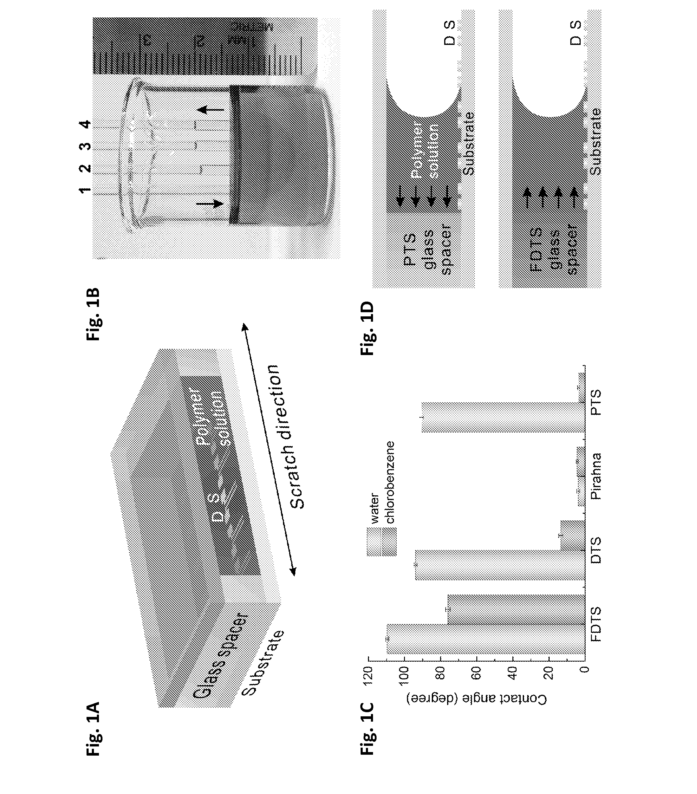
[0064]A sandwich tunnel system is provided, which is separated by functionalized glass spacers to induce capillary action for controlling the polymer nanostructure, crystallinity, and charge transport. Using capillary action, saturation mobilities with average values of 21.3 cm2V−1 s−1 and 18.5 cm2V−1 s−1 have been demonstrated on two different semiconducting polymers at a transistor channel length of 80 μm. These values are limited by the source-drain contact resistance, Rc. Using a longer channel length of 140 μm where the contact resistance is less important, μh=36.3 cm2V−1 s−1 was measured. Extrapolating to infinite channel length where Rc is unimportant, the intrinsic mobility for PCDTPT (Mn=140 kDa) at this degree of chain alignment and structural order is μh=36.3 cm2V−1 s−1. These results demonstrate a pathway towards high performance, solution processable, and low-cost organic electron...

example 2

Atomic Force Microscopy of Polymer Films

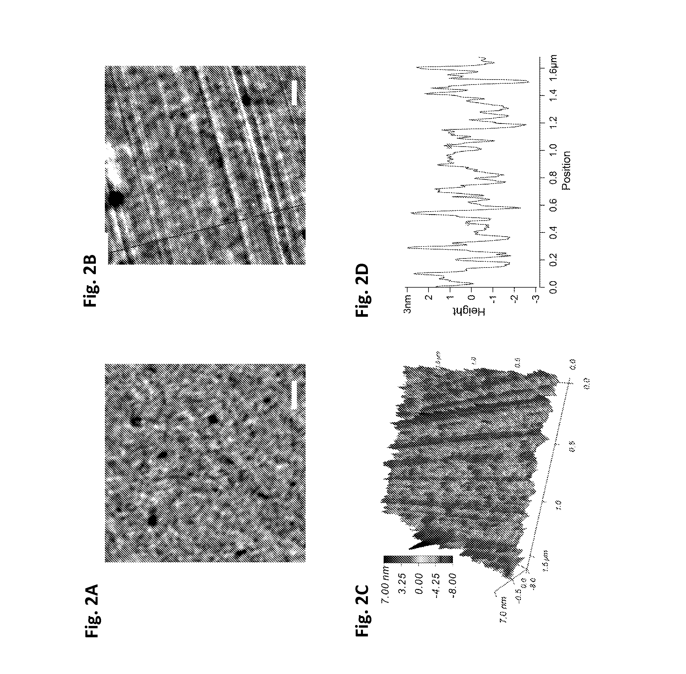
[0069]To investigate how the strength of capillary action can affect the polymer alignment on the textured substrate, atomic force microscopy (AFM) in tapping mode was performed to examine and compare the nanomorphology on the bottom surfaces of polymer films (see the details for sample preparation in Example 6), prepared using two opposite treatments (FDTS and PTS) to the spacers in the sandwich systems, using identically nano-grooved Si / SiO2 substrates. The donor-acceptor copolymer, poly[4-(4,4-dihexadecyl-4H-cyclopenta[1,2-b:5,4-b′]dithiophen-2-yl)-alt-[1,2,5]thiadiazolo[3,4-c]pyridine] (PCDTPT, Mn=140 kDa) was used to prepare the solution [27].

[0070]FIGS. 2A and 2B show the AFM topographic images of the bottom surfaces (taken from areas approaching the spacers) of two deposited films prepared using the spacers with FDTS treatment and PTS treatment, respectively. The film prepared using FDTS-treated spacers exhibits featureless surfaces and...

example 3

Grazing Incidence Wide Angle X-Ray Scattering of Films

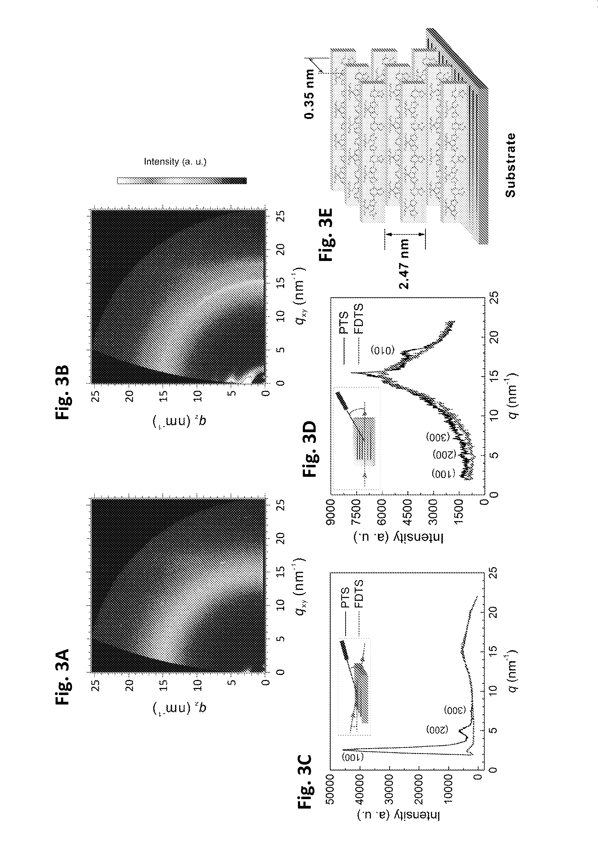
[0071]As the AFM analysis is limited to the surface morphology, to gain deeper insight into the molecular packing and crystallinity in the deposited films, measurements by grazing incidence wide angle X-ray scattering (GIWAXS) were conducted on the deposited films. Several noticeable changes in the polymer microstructure are observed in the 2D GIWAXS patterns for the films prepared using FDTS-treated spacers and PTS-treated spacers, as shown in FIGS. 3A and 3B, respectively. Only minor first-order lamellar scattering can be observed in FIG. 3A, indicating the lack of long-range order; the film prepared using FDTS-treated spacers is essentially amorphous. By contrast, the pattern of the film, prepared using PTS-treated spacers exhibits numerous diffraction features. One can observe (100), (200) and (300) scattering peaks, consistent with aligned polymer chains, and clear indication of π-π interchain stacking (FIG. 3B). The X-ray s...


PUM

PropertyMeasurementUnit
Angleaaaaaaaaaa
Angleaaaaaaaaaa
Volumetric flow rateaaaaaaaaaa

Abstract

Embodiments of the invention include methods and materials for preparing organic semiconducting layers, for example one used in an organic semiconductor device including a substrate with a nanostructured surface and a polymeric semiconductor film overlying the nanostructured surface. Aspects of the invention use capillary action to modulate polymer chain self-assembly on a surface and unidirectional alignment at a critical buried interface where charge carriers migrate between a dielectric and the polymer. By controlling the properties of the surfaces upon which polymers are disposed, artisans can enhance the transistor saturated mobilities of conjugated polymers.

Description

REFERENCE TO RELATED APPLICATIONS[0001]This application claims the benefit under 35 U.S.C. Section 119(e) of co-pending U.S. Provisional Patent Application Ser. No. 61 / 923,452, filed on Jan. 3, 2014, entitled “HIGH MOBILITY POLYMER THIN FILM TRANSISTORS WITH CAPILLARITY MEDIATED SELF-ASSEMBLY”, the contents of which are incorporated herein by reference.TECHNICAL FIELD[0002]The invention relates to methods and materials useful in organic semiconductor devices.BACKGROUND OF THE INVENTION[0003]There is great interest in a new generation of electronic devices which use organic semiconductors as their active components, such as organic light-emitting transistors (OLETs) and organic photovoltaics (OPVs). In particular, there is interest in conjugated polymer based organic semiconductors because they combine the electrical properties of semiconductors with the mechanical properties of plastics. Furthermore, since these materials can be processed relatively inexpensively with techniques suc...

Claims


Application Information

Patent Timeline
IPC IPC(8): H01L51/00B05C9/02
CPCH01L51/0003H01L51/0036H01L51/0035B05C9/02H10K71/191H10K85/113H10K85/151
Inventor LUO, CHANHEEGER, ALAN
Owner RGT UNIV OF CALIFORNIA
Why Eureka
Try Eureka