Indium gallium zinc oxide layers for thin film transistors

a thin film transistor and zinc oxide technology, applied in semiconductor devices, chemical vapor deposition coatings, coatings, etc., can solve the problems of limited stoichiometries of pvd igzo films, limited speed of pvd igzo process development, and difficult design requirements, so as to improve throughput and production

Inactive Publication Date: 2015-08-06
APPLIED MATERIALS INC
View PDF5 Cites 25 Cited by
  • Summary
  • Abstract
  • Description
  • Claims
  • Application Information

AI Technical Summary

Benefits of technology

[0016]Embodiments of the disclosure may provide methods for forming portions of a TFT device using a cluster tool-integrated (in-situ) process to form a three-layer gate dielectric-IGZO-top dielectric stack and other such mul

Problems solved by technology

These trends have resulted in challenging design requirements for the formation of thin film transistors (TFTs) that can meet these needs.
Each of the described methods of depositing an IGZO layer has its own set of challenges and problems.
First of all, PVD IGZO films are limited to the stoichiometries of the PVD targets, which are manufactured and used to form TFTs with considerable investments of money and time for a researcher studying a new stoichiometric combination of IGZO film.
This not only limits the speed of PVD IGZO process development, but limits complexity of a practically deposited structure.
A PVD stoichiometric bi-layer process can require two separate PVD chambers, which is more expensi

Method used


Image

  • Indium gallium zinc oxide layers for thin film transistors
  • Indium gallium zinc oxide layers for thin film transistors
  • Indium gallium zinc oxide layers for thin film transistors

Examples


Embodiment Construction

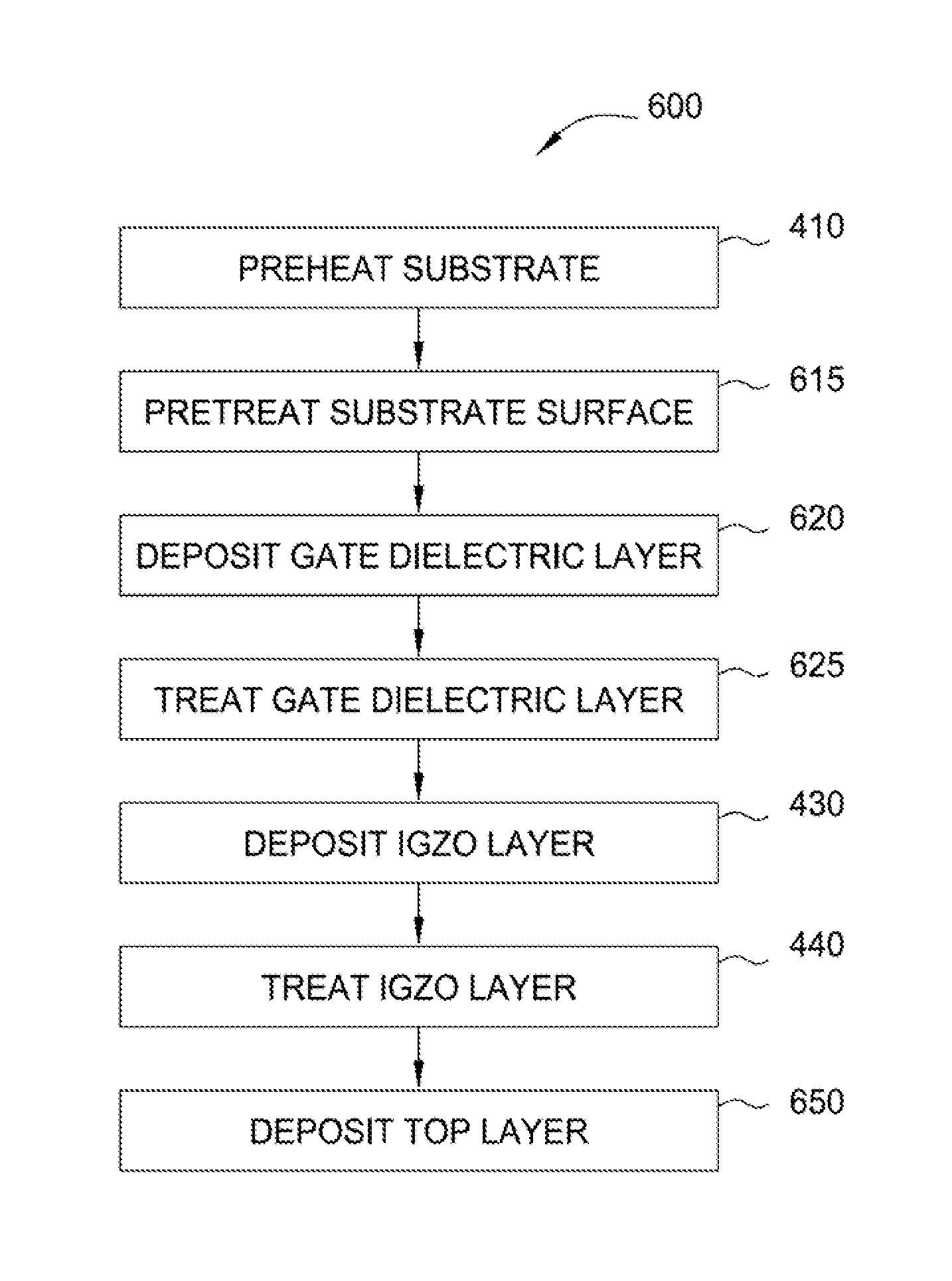
[0025]The present disclosure generally provides methods for forming an IGZO active layer within a thin film transistor (TFT) device. However, it should be understood that the embodiments disclosed herein may have utility in system configurations other than those shown in the illustrative examples of the disclosure, and that these embodiments may also find applications which are not related to displays or display TFTs, for example, integrated circuits, micro-electro-mechanical systems (MEMS) and solar panels. Embodiments of the disclosure may also find utility in processes not directly detailed in this disclosure, such as plasma etching and layer treating processes.

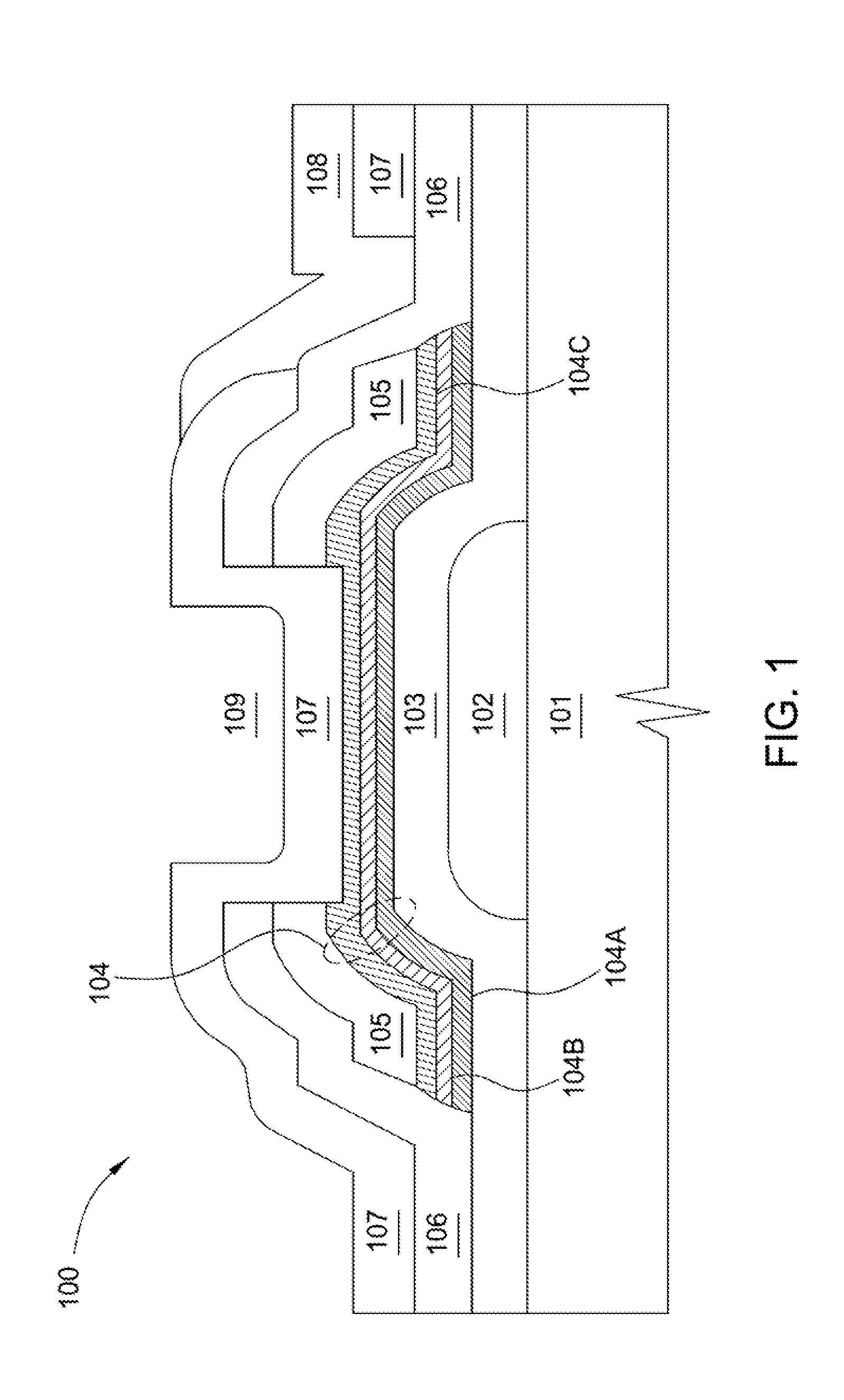
[0026]FIG. 1 is a cross-sectional diagram for a bottom-gate TFT device 100 that is formed on a substrate 101. A substrate 101 for liquid crystal display (LCD) or organic light emitting diode (OLED) applications is typically transparent and rectangular. One popularly used material is glass. Glass display substrate sheets sp...


PUM

PropertyMeasurementUnit
Dielectric polarization enthalpyaaaaaaaaaa
Electrical conductivityaaaaaaaaaa
Ratioaaaaaaaaaa

Abstract

Embodiments of the present disclosure generally provide a method and apparatus for forming an IGZO active layer within a thin film transistor (TFT) device. In one embodiment, a method is provided for forming an IGZO active layer on a dielectric surface using a PECVD deposition process. In one embodiment, a method is provided for pretreating and passivating the dielectric surface for receiving the PECVD formed IGZO layer. In another embodiment, a method is provided for treating a PECVD formed IGZO layer after depositing said layer. In another embodiment, a method is provided for forming a multi-layer or complex layering structure of IGZO, within a PECVD processing chamber, for optimizing TFT electrical characteristics such as carrier density, contact resistance, and gate dielectric interfacial properties. In yet another embodiment, a method is provided for forming integrated layers for a TFT including IGZO within an in-situ environment of a cluster tool.

Description

CROSS-REFERENCE TO RELATED APPLICATIONS[0001]This application claims benefit of U.S. Provisional Patent Application Ser. No. 61 / 936,276 (APPM / 21586L), filed Feb. 5, 2014, which is incorporated herein by reference.BACKGROUND OF THE DISCLOSURE[0002]1. Field[0003]Embodiments of the disclosure generally relate to a method and apparatus for forming a thin film transistor device.[0004]2. Description of the Background Art[0005]Several trends in the evolution of flat screen displays are larger screen sizes, smaller pixels, LED-based pixels, and reduced display power consumption. These trends have resulted in challenging design requirements for the formation of thin film transistors (TFTs) that can meet these needs. Because Indium Gallium Zinc Oxide (IGZO) can be made with a carrier mobility 20-50 times greater than that of amorphous silicon, TFTs with IGZO channels can be made smaller, more transparent and less power-consuming than TFTs with amorphous silicon channels.[0006]TFTs can be form...

Claims


Application Information

Patent Timeline
IPC IPC(8): H01L21/02
CPCH01L21/02565H01L21/02488H01L21/0262H01L21/02472H01L21/02483H01L21/02554C23C16/407C23C16/45574C23C16/5096H01L29/66969H01L29/7869H01L29/78693H01L29/78696
Inventor WON, TAE KYUNGWHITE, JOHN M.CHOI, SOO YOUNG
Owner APPLIED MATERIALS INC
Why Eureka
Try Eureka