High contrast surface marking using nanoparticle materials

a technology of nanoparticles and materials, applied in the direction of inks, nuclear engineering, transportation and packaging, etc., can solve the problems of insufficient time factor and energy consumption, inability to use a kiln, process, etc., and achieve the effect of strong bonding and better color properties

Active Publication Date: 2015-12-03
HARRISON FAMILY TRUST
View PDF5 Cites 11 Cited by
  • Summary
  • Abstract
  • Description
  • Claims
  • Application Information

AI Technical Summary

Benefits of technology

[0018]Most properties of nanoparticles are size dependent and do not become apparent until the size has been reduced to the nanometer scale. The high surface to volume ratio coupled with the size effects (quantum effects) of such nanoparticles introduces many size-dependent phenomena, including new or improved physical, chemical and mechanical properties. Examples of such phenomena are the increased specific surface area facilitating the absorption and / or scattering of visible light and laser, diode or other radiant energy, as well as the decreased melting point of bulk particulate materials when their particle size is reduced to the nanometer scale.
[0053]Further embodiments include systems and methods as described above, wherein the laser marking or inkjet printing system is capable of the rapid placement of a durably cured and / or bonded color image or other graphic directly onto the surface of a substrate of metal, glass, ceramic, porcelain, natural or engineered stone, as well as plastic and polymer composites or other organic materials with high resolution and high contrast.

Problems solved by technology

One problem with these processes is that the time factor and energy consumption are not commercially efficient enough to make the marking or decoration process economically feasible in smaller quantities.
Furthermore, these processes, requiring a kiln, do not lend themselves to portability.
This method cannot be used on glass, ceramic, porcelain or other brittle materials because of potential surface damage and / or breakage.
Where used, the method produces a relatively low-resolution, fast and permanent mark; however, color and high-contrast marking cannot be achieved.
This method produces high-resolution and high-contrast marks or decorations with color, if desired, and is relatively fast, but lacks real long term durability.
These organic resin or polymer binder systems usually comprise a monomer, oligomer, photopolymerization initiator and various additives (stabilizers, fillers, pigments, etc.) and are used with an ultraviolet lamp curing step which is relatively time consuming; however, even with the use of solvents and ultraviolet curing there remains a lack of long term durability to abrasion, outdoor weather and sunlight conditions.
The resulting mark or decoration is only as durable as the polymer material or coating, but lacks long term ultraviolet stability.
What would appear ironic is that the changes in the physical properties of nanoparticles with size are not always predictable or desirable.
For example, ferromagnetic materials smaller than 10 nm can switch their magnetization direction using room temperature thermal energy, thus making them unsuitable for electronic memory storage applications.
Moreover, comminution of the pigment by contact with the milling media results in pigment surfaces exhibiting a high number of surface asperities, a large variation in particle size, and significant variations in particles and their properties from batch to batch.
Furthermore, contamination of the dispersions from the mechanical parts of the milling equipment can result due to the intimate contact of the pigment with the milling media.

Method used


Image

  • High contrast surface marking using nanoparticle materials
  • High contrast surface marking using nanoparticle materials
  • High contrast surface marking using nanoparticle materials

Examples


Embodiment Construction

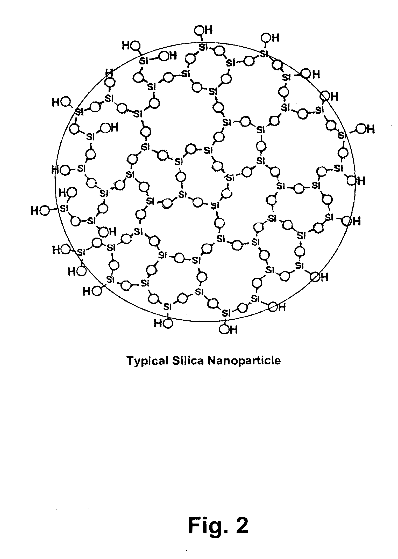
[0066]Physical and chemical changes induced by mechanical means during the milling processes described above can cause significant increases in the surface areas of the basic glass, ceramic, clay, metal, metal chromate, metal tungstate and metal molybdate and other metallic, organometallic, inorganic or organic compounds, materials, dispersions and solutions or combinations thereof according to the BET data. An estimation of the mean particle sizes using the BET, SEM and XRD data indicates a decrease from approximately 1 micron to the approximate 10-200 nm range and is most likely explained by the smaller primary crystallites of the elemental metals and / or other metallic, organic or inorganic materials and compounds. The solution or colloidal suspension structure confirms that the compositions contain discrete anions, cations and / or water molecules, connected through hydrogen bonds. In fact, the unique and distinguishing features of these compositions and substances are their extens...


PUM

PropertyMeasurementUnit
sizesaaaaaaaaaa
particle sizesaaaaaaaaaa
temperaturesaaaaaaaaaa

Abstract

Methods and compositions are disclosed for quickly creating durable surface marks and / or decorations on substrates including metal, glass, ceramic, porcelain, natural and engineered stone, as well as plastics, polymer composites and other organic materials with color, high resolution and high contrast using inkjet technology and laser, NIR diode or UV LED energy. The improved methods and compositions are based on established and emerging sub-micron and nanoparticle technology. Most properties of nanoparticles are size dependent and do not become apparent until the particle size has been reduced to the nanometer scale. Examples of such properties include increased specific surface area, facilitating the absorption and / or scattering of visible light and laser, NIR diode or UV LED energy and the decreased melting point of such materials when their particle size is reduced to the nanometer scale. Improved results such as smoothness and durability are obtained by using nanoparticles of silica, pigments and other materials in such marking processes.

Description

REFERENCE TO RELATED APPLICATIONS[0001]This application claims the benefit of my provisional applications U.S. Ser. No. 61 / 997,220, filed May 27, 2014 for “METHODS AND COMPOUNDS FOR QUICKLY CREATING PERMANENT COLOR SURFACE MARKS AND / OR DECORATIONS ON METAL, GLASS, CERAMIC, PORCELAIN, NATURAL AND ENGINEERED STONE, AS WELL AS PLASTIC AND POLYMER COMPOSITE MATERIALS WITH HIGH-RESOLUTION AND HIGH-CONTRAST USING LASER OR DIODE ENERGY,” and U.S. Ser. No. 62 / 176,129, filed Feb. 9, 2015 for “METHODS AND COMPOUNDS FOR QUICKLY CREATING DURABLE, COLOR SURFACE MARKS AND / OR DECORATIONS ON METAL, GLASS, CERAMIC, PORCELAIN, NATURAL AND ENGINEERED STONE, AS WELL AS PLASTIC, POLYMER COMPOSITE AND OTHER ORGANIC MATERIALS WITH HIGH-RESOLUTION AND HIGH-CONTRAST USING LASER OR DIODE ENERGY.”BACKGROUND[0002]1. Field of the Invention[0003]The present subject matter relates to improvements to existing marking materials and compositions for use in marking operations in conjunction with commercially availabl...

Claims


Application Information

Patent Timeline
Patent Type & Authority Applications(United States)
IPC IPC(8): C09D11/36C09D11/02B05D3/06C09D11/322
CPCC09D11/36C09D11/322Y10T428/24893B05D3/065C09D11/02B05D3/067B41M5/262B41M5/267B41M2205/04
Inventor HARRISON, PAUL W.
Owner HARRISON FAMILY TRUST
Why Eureka
Try Eureka